Capillary coating method

Inactive Publication Date: 2005-03-31
OSRAM OPTO SEMICON GMBH & CO OHG
View PDF8 Cites 27 Cited by
  • Summary
  • Abstract
  • Description
  • Claims
  • Application Information

AI Technical Summary

Benefits of technology

[0011] It is another object of the present invention to provide a method of depositing material on a substrate, using capillary forces, that allows quicker deposition than using an inkjet method.
[0012] It is another object of the present invention to provide a method of depositing material on a substrate, using capillary forces, that results in spatial resolution that is greater than if a flexographic printing method were used.
[0013] It is another object of the present invention to provide a method of depositing material on a substrate, using capillary forces, that results in spatial resolution that is greater than if a screen printing method were used.
[0015] A spacer / pattern layer is coated onto the substrate upon which a film of material is desired. A cover layer is then placed in contact with the spacer / pattern layer. Pressure is applied and the spacer / pattern layer is held between the substrate and the cover layer, forming a multilayered structure. At least one edge of the multilayered structure is dipped into a solution containing the desired material for deposition. Advantageously, the capillary action draws solution into the multilayered structure. The solution is allowed to dry and a patterned film remains once the cover layer is removed. If desired, the process may be repeated with different solutions. Advantageously, different edges of the multilayered structure and / or multilayered structures having the same substrate but different spacer / pattern layers may be used to facilitate subsequent deposition of additional solutions.

Problems solved by technology

A disadvantage of inkjet printing is that it is limited in speed.
Such adjustments require additional expense and often slow down the printing process.
Even if the printing process is not appreciably slowed down, the multiple print cartridges or arrays of nozzles may not provide enough additional speed to the printing process.
Both these methods have the disadvantages of having limited spatial resolution and, since the processes involve the mechanism of application touching the surface of the substrate, there is increased likelihood of contamination.

Method used


Image

  • Capillary coating method
  • Capillary coating method
  • Capillary coating method

Examples


example application

[0044] Example Application

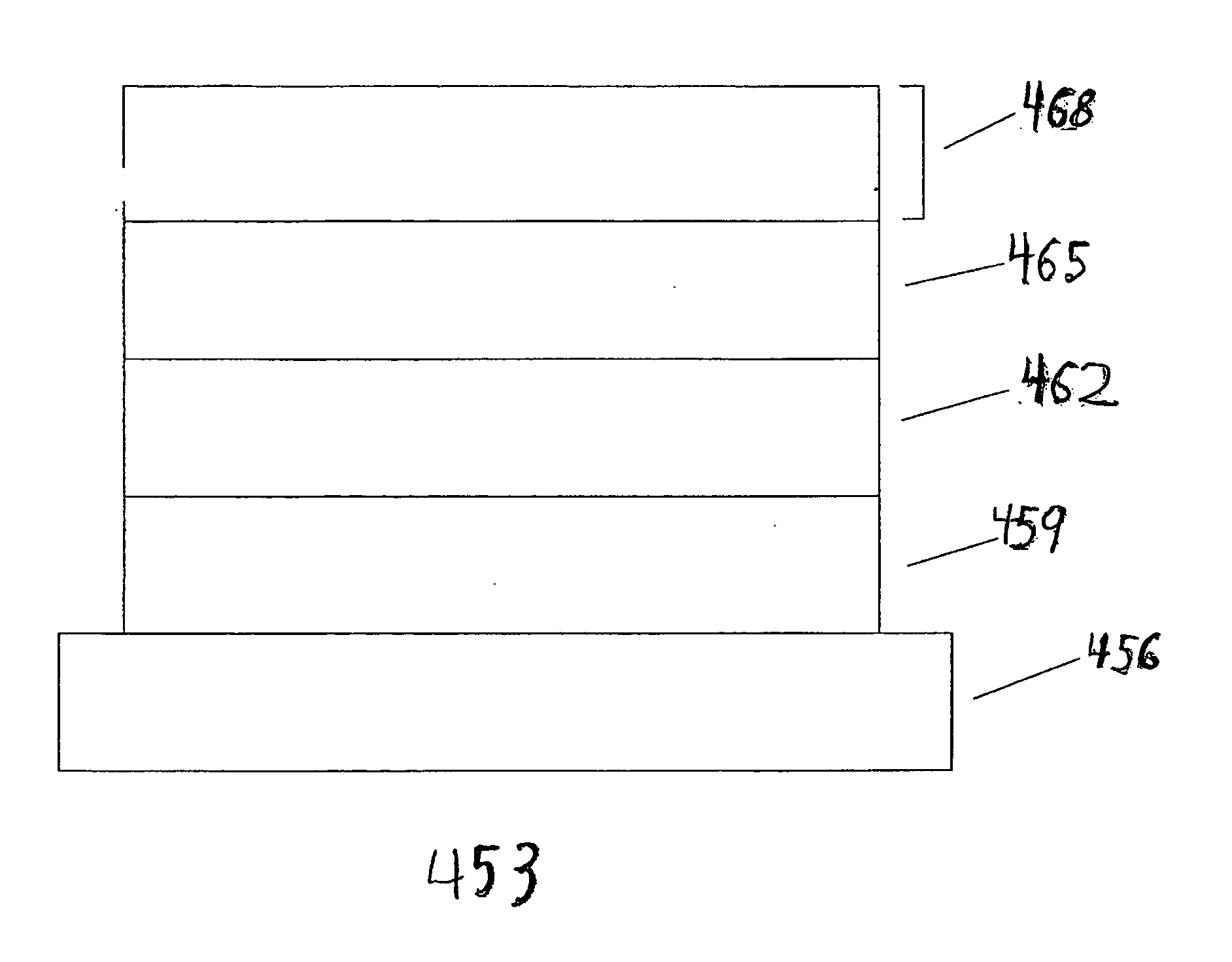
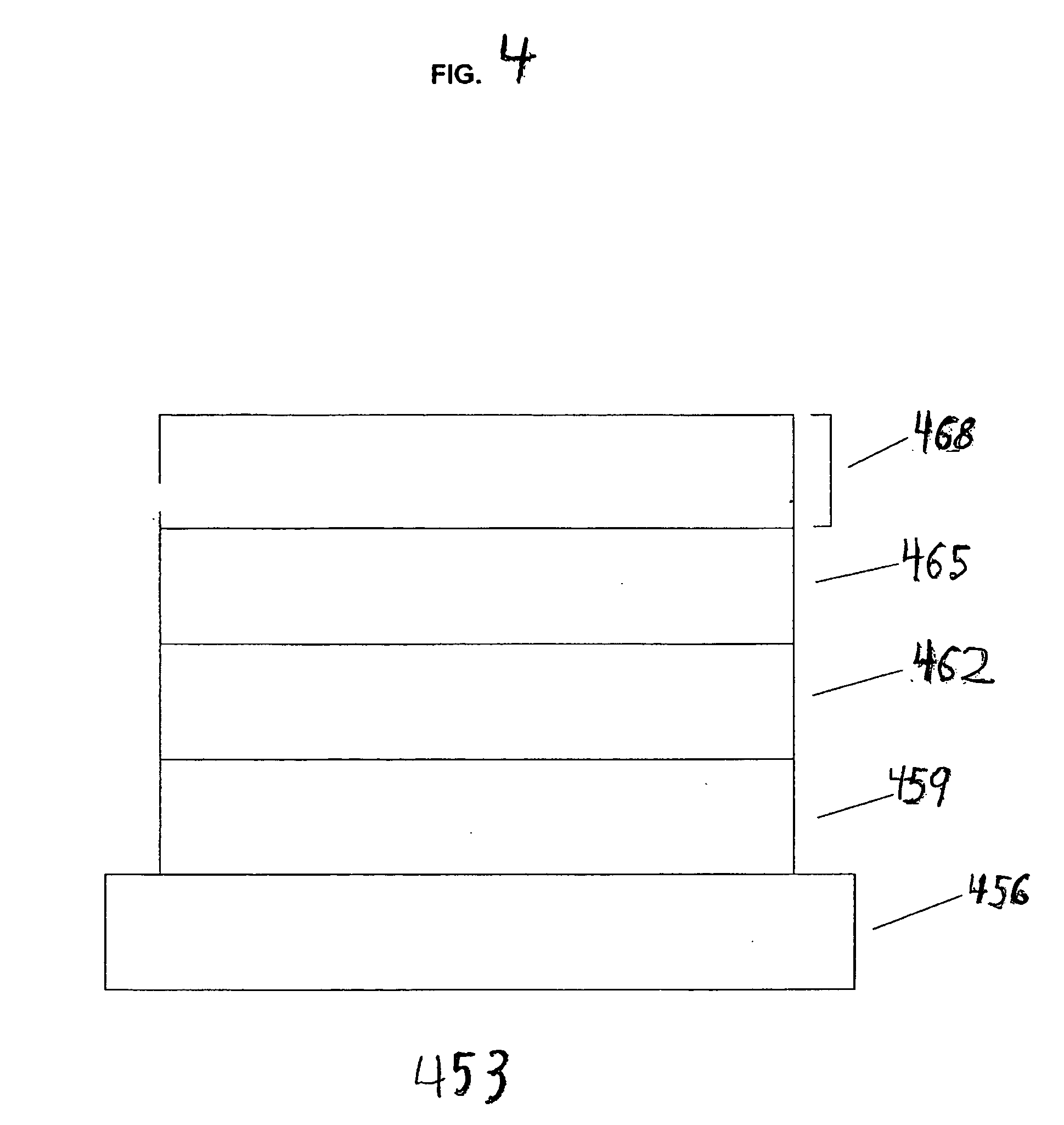
[0045] A specific example of an electronic device is an OLED. FIG. 4 shows an embodiment of an OLED 453 according to the present invention. The OLED 453 includes a substrate 456 that may be comprised of, for example, glass or plastic. The OLED 453 also includes a first electrode such as an anode layer 459 that is deposited on the substrate 456. The anode layer 459 may be, for example, indium tin oxide (“ITO”). The OLED 453 also includes at least one semiconductor layer, preferably, two organic layers: a conducting polymer layer 462 that is deposited on the anode layer 459, and an emissive polymer layer 465 that is deposited on the conducting polymer layer 462. The conducting polymer layer 462 assists in injecting and transporting holes. The emissive polymer layer 465 assists in injecting and transporting electrons. In one configuration of this embodiment, the emissive polymer layer 465 emits light. In another configuration, another separate layer is deposit...


PUM


Abstract

Material is deposited on a substrate layer by forming a multilayered structure and dipping the multilayered structure into a solution containing the material for a sufficient length of time to allow the solution to spread through capillary action to a predetermined region. The multilayered structure is formed by coating the substrate layer with a spacer / pattern layer that defines the predetermined region and pressing a cover layer against the space / pattern layer.

Description

BACKGROUND OF THE INVENTION [0001] 1. Field of the Invention [0002] The present invention relates to the deposition of materials on substrates. More particularly, the present invention relates to making use of capillary action to coat substrates. [0003] 2. Description of Related Art [0004] Electronic devices such as information displays, large area sensors, planar light sources, solar cells and circuitry composed of organic semiconducting materials require the precise placement of materials between and around conducting electrodes, usually composed of metals. The films deposited on the substrate range in thickness from several nanometers to tens of micrometers. A common requirement is the deposited materials must be uniform in thickness across the substrate. Another requirement is the need for precise spatial deposition of the materials. Such devices typically include a pair of electrodes (e.g., an anode and a cathode) with at least one semiconductive layer between the electrodes. O...

Claims


Application Information

Patent Timeline
IPC IPC(8): B32B7/06H01L51/00H01L51/40
CPCB05D1/00H01L51/0003B32B7/06Y10T428/31504H10K71/12
Inventor GUPTA, RAHULCARR, JOSEPH
Owner OSRAM OPTO SEMICON GMBH & CO OHG
Why Eureka
Try Eureka