
Low profile carrier for non-wafer form device testing

a low-profile carrier and non-wafer-form technology, applied in the direction of testing circuits, resistance/reactance/impedence, instruments, etc., can solve the problems of easy displacement of location, poor die marking, and easy displacement of location in clearan

Inactive Publication Date: 2005-03-17
ATMEL CORP
View PDF7 Cites 5 Cited by
  • Summary
  • Abstract
  • Description
  • Claims
  • Application Information

AI Technical Summary

Benefits of technology

[0010] The present invention accomplishes this by providing a low-profile carrier for temporarily mounting a non-wafer form device. The low-profile carrier holds the non-wafer form device (e.g., an integrated circuit chip, a thin film head structure, one or more molded array packages, etc.) magnetically into recesses which are machined or otherwise formed in the low-profile carrier.
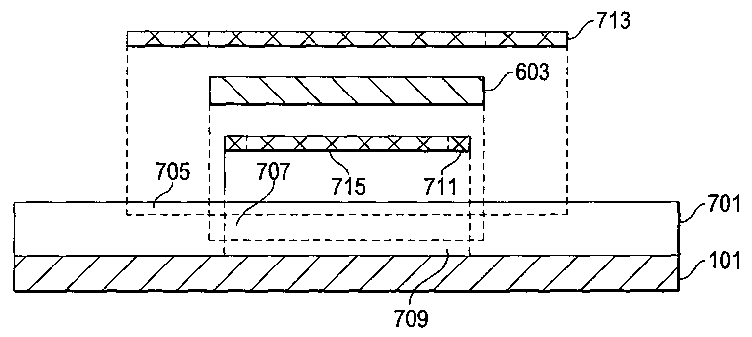
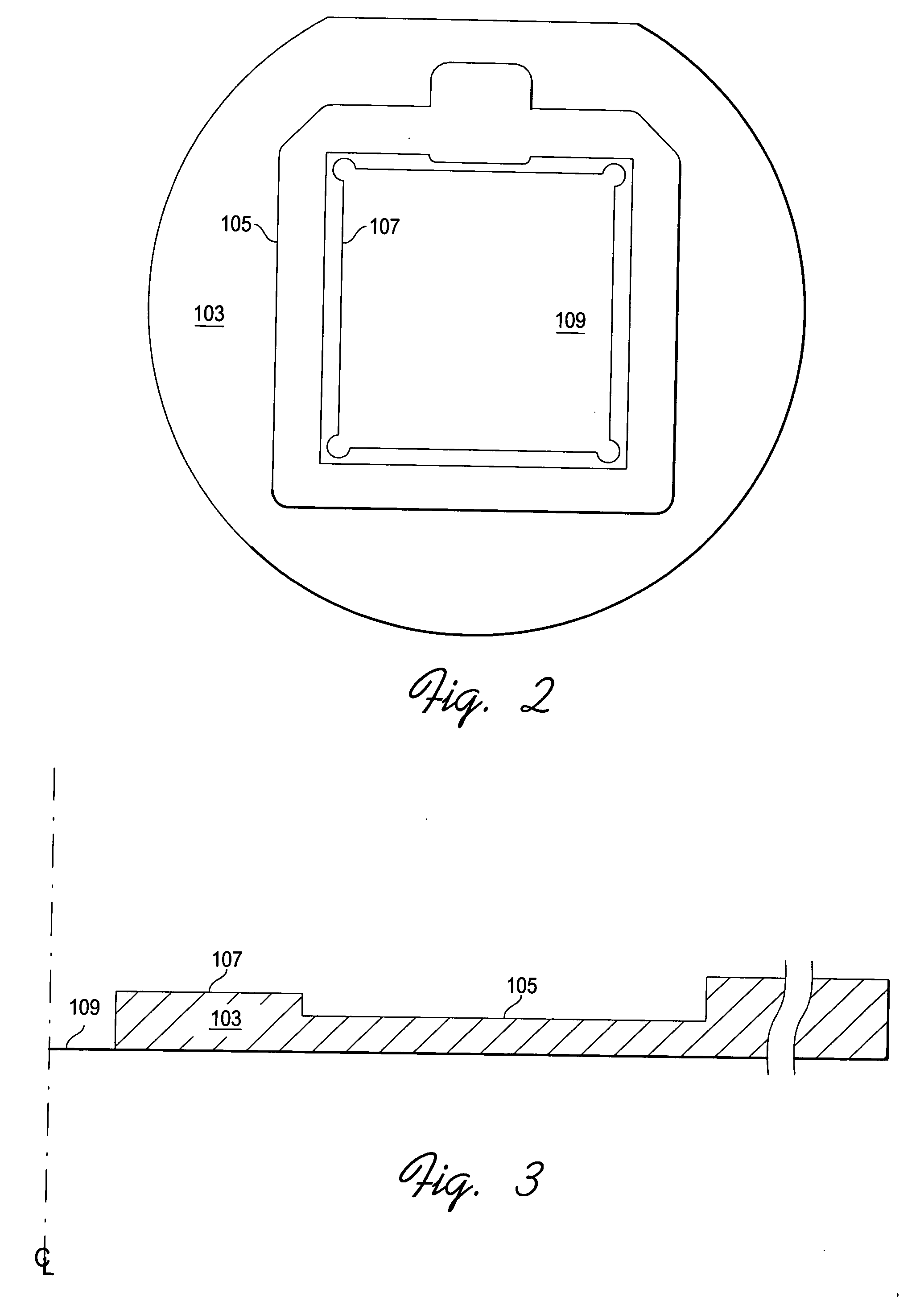
[0011] In one embodiment, the low-profile carrier comprises a test ring holder configured to hold the non-wafer form device. The test ring holder is configured to be bonded to a mechanical support base, for example, a thinned semiconductor wafer. A test ring magnet with a thru-hole is configured to be mounted substantially within a first recess formed on the top of the test ring holder and a concentric second recess machined within the first recess forms a mounting location for the non-wafer form device. Finally, a test ring cover is configured to hold the non-wafer form device magnetically within the test ring holder.
[0012] In an alternative embodiment, a low-profile carrier comprises a test ring holder configured to hold said non-wafer form device. The test ring holder is additionally configured to be mechanically coupled to a support base. A test ring cover with a thru-hole is configured to be held magnetically in a location proximate to the test ring holder and is mounted substantially within a first recess formed within the top of the test ring holder. A second recess is concentrically machined in the first recess and forms a mounting location for the non-wafer form device.
[0013] In another alternative embodiment, a low-profile carrier comprises a test ring holder configured to hold the non-wafer form device. The test ring holder is additionally configured to be mechanically coupled to a support base. A test ring cover with a thru-hole is configured to be held magnetically in a location proximate to the test ring holder and to be mounted substantially within a first recess formed within the top of the test ring holder. A second recess is concentrically machined in the first recess and forms a mounting location for the non-wafer form device. A thru-hole is formed within the test ring holder and circumscribed within the second recess. Finally, an insert configured to be mounted within the thru-hole is coupled to the support base and serves to be magnetically attracted to the test ring cover, thereby holding the non-wafer form device in place.

Problems solved by technology

If the test fails the die is marked as bad.
As a result, the electrodes on the bare chip and the contact terminals on the testing substrate cannot be aligned with good precision.
In addition, since a clearance to connect the testing substrate and the bare chip resides, displacement in location is easy to be caused in the clearance.
Additionally, standard wafer-probe testers are limited to testing wafers due to several factors.
However, this solution presents several problems.
Some devices are not suitable for modification due to size constraints (e.g., an overall thickness will b too great when mounted or otherwise affixed to a suitable carrier substrate).
Other devices will sacrifice yield by discarding good devices while attempting to accommodate to a standard wafer size (e.g., a large molded array package (MAP) will lose peripheral devices when the MAP is modified into a wafer form).
Still other devices are not compatible with standard vacuum transport tools (such as vacuum end-effectors on robotic transport arms).

Method used


Image

  • Low profile carrier for non-wafer form device testing
  • Low profile carrier for non-wafer form device testing
  • Low profile carrier for non-wafer form device testing

Examples


Embodiment Construction

[0021] The present invention will now be described with reference to preferred embodiments thereof. FIG. 1 shows an exemplary embodiment of a low-profile carrier 100. The low-profile carrier generally includes a semiconductor wafer support 101, a test ring holder 103 with a first recess 105, a second recess 107, and an optional thru-hole 109, a test ring magnet 111, and a test ring cover 113. A non-wafer form device (e.g., an integrated circuit chip, a thin film head structure, one or more molded array packages, etc.—not shown) is placed between the test ring magnet 111 and is held in place by the test ring cover 113. The low-profile carrier with the mounted non-wafer form device may then be placed into, for example, a wafer boat to allow the non-wafer form device to be loaded by an automated test machine, such as a wafer-prober.

[0022] The semiconductor wafer support 101 serves as a mechanical support base for the test ring holder 103. Using a semiconductor wafer as a support base ...


PUM


Abstract

The present invention allows non-wafer form devices to be tested on a standard automatic wafer-probe tester or other automated test or measurement device commonly employed in semiconductor or allied industries (e.g., flat panel display, data storage, or the like) processes. The present invention accomplishes this by providing a low-profile carrier for temporarily mounting a non-wafer form device. The low-profile carrier holds the non-wafer form device (e.g., an integrated circuit chip, a thin film head structure, one or more molded array packages, etc.) magnetically into recesses which are machined or otherwise formed in the low-profile carrier.

Description

TECHNICAL FIELD [0001] The present invention relates to a test carrier for a semiconductor integrated circuit. More particularly, the present invention relates to a test carrier for holding a semiconductor integrated circuit, or the like, in non-wafer form for testing on an automated wafer probe tester or other piece of test or metrology equipment. BACKGROUND ART [0002] Integrated circuit (IC) manufacturers produce die on typically circular substrates referred to as wafers. A wafer may contain hundreds of individual rectangular or square die. Die on wafer, or unsingulated die, must be tested to determine good from bad before the dies are singulated. Unsingulated die testing traditionally occurs by physically probing each die at the die pads, which allows a tester connected to the probe to determine good or bad die. [0003] Conventional die testing is performed using a tester and pad probe assembly. The probe assembly is positioned over a selected die and lowered to make contact with ...

Claims


Application Information

Patent Timeline
Patent Type & Authority Applications(United States)
IPC IPC(8): H01L21/673H01L21/687
CPCG01R1/0483H01L21/68785H01L21/68778H01L21/67346
Inventor LAM, KEN M.KOVATS, JULIUS A.
Owner ATMEL CORP
Learn More