Superconductor semiconductor integrated circuit
a superconductor semiconductor and integrated circuit technology, applied in the field of superconducting circuits, can solve the problems of difficult timing calibration with the later-stage circuit, difficult high-speed demultiplexing of data signals, and inability to directly transmit sfq pulses from the sfq circuit to the semiconductor circuit, etc., to achieve the effect of easy transmission of data signals
- Summary
- Abstract
- Description
- Claims
- Application Information
AI Technical Summary
Benefits of technology
Problems solved by technology
Method used
Image
Examples
embodiment 1
[0043] (Embodiment 1)
[0044] In Embodiment 1, the overall construction and operation of an A / D converter will be described. The detailed construction and operation of components will be then described.
[0045] (The Overall Construction of an A / D Converter)
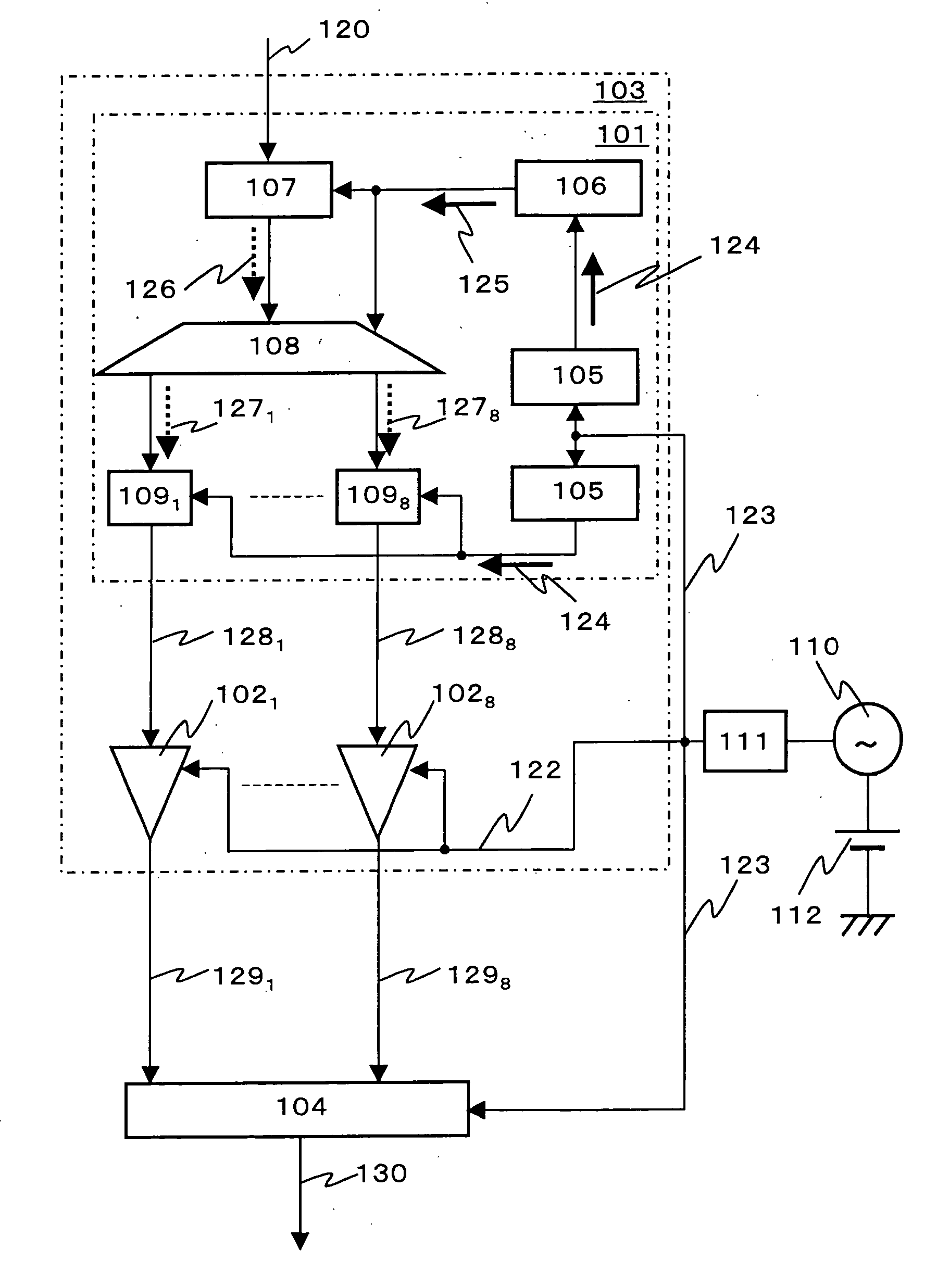
[0046]FIG. 1 is a diagram showing the overall construction of an A / D converter according to Embodiment 1. The converter has a superconducting front-end circuit 103 having an SFQ front-end circuit 101 and a superconducting amplifier circuit 102, and a semiconductor back-end circuit 104. The superconducting front-end circuit 103 oversamples an analog input signal 120, converts the analog signals to the digital data signals and makes the frequency and the voltage level of the data signals transmittable to the semiconductor back-end circuit 104. The semiconductor back-end circuit 104 signal-processes a voltage data signal 129 of the superconducting front-end circuit 103 to generate a final digital data signal 130.
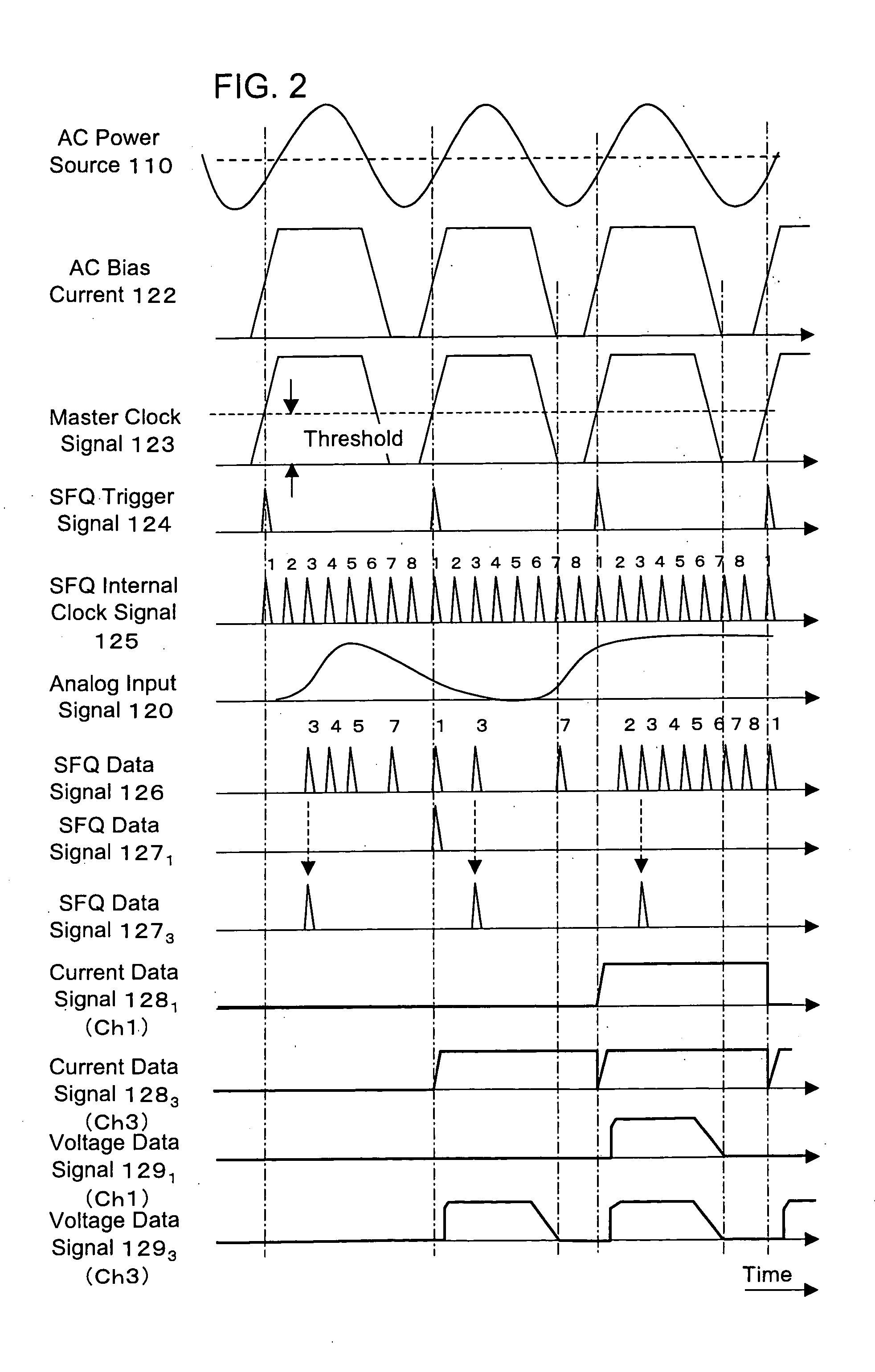
[0047]FIG. 2 is a diag...
embodiment 2
[0104] (Embodiment 2)
[0105]FIG. 13 is a block diagram showing, as Embodiment 2, a circuit construction when using the ring oscillator circuit 250 for the clock signal frequency multiplier circuit 106. A specific example of the ring oscillator circuit 250 is proposed in FIG. 5 of Patent Document 2. The bias current I124 supplied to the ring oscillator circuit 250, as in the 2N-bit ladder-type clock signal generating circuit 201 described in FIG. 4, is connected to the junctions of all bias current sources shown in the ring oscillator circuit 250 via the bias resistance. Here, for simplifying the drawing, the bias current I124 is introduced by the arrow. When one SFQ signal is generated by the SFQ generating circuit 105 to be inputted to the ring oscillator circuit 250, the SFQ signal is circulated on the JTL arranged in the ring form to generate an infinite number of SFQ pulse trains from the SP at any point. The pulse train is used as the SFQ internal clock signal 125. The construct...
embodiment 3
[0110] (Embodiment 3)
[0111] The memory circuit 109 and the superconducting amplifier circuit 102 of the AC-biased latching circuit described in FIG. 11 of Embodiment 1 can increase the output voltage. The AC bias current supplied to the latching circuit affects the operation of the SFQ circuit due to cross talk. FIG. 14 is an equivalent circuit diagram showing the constructions of the memory circuit 109 and the superconducting amplifier circuit 102 devised to solve-the problem of cross talk of the AC-biased latching circuit due to the AC bias current. FIG. 15 is a diagram showing an example of the layout of the main part of the circuits shown in FIG. 14. FIG. 16 is a diagram of assistance in explaining the component devices of FIG. 15.
[0112] As the circuit shown in FIG. 14 can be understood by comparison with FIG. 11, in the memory circuit 109 and the superconducting amplifier circuit 102 of Embodiment 3, a pair of the memory circuit 1091 and the superconducting amplifier circuit 1...
PUM
 Abstract
Description
Claims
Application Information
 - R&D
- Intellectual Property
- Life Sciences
- Materials
- Tech Scout
- Unparalleled Data Quality
- Higher Quality Content
- 60% Fewer Hallucinations
Browse by: Latest US Patents, China's latest patents, Technical Efficacy Thesaurus, Application Domain, Technology Topic, Popular Technical Reports.
© 2025 PatSnap. All rights reserved.Legal|Privacy policy|Modern Slavery Act Transparency Statement|Sitemap|About US| Contact US: help@patsnap.com


