
Electron beam enhanced large area deposition system

a deposition system and large area technology, applied in the direction of electrolysis components, vacuum evaporation coatings, coatings, etc., can solve the problems of poor target utilization, waste of target materials, and lower growth rate, and achieve the effect of improving process control

Inactive Publication Date: 2005-02-24
THE UNITED STATES OF AMERICA AS REPRESENTED BY THE SECRETARY OF THE NAVY
View PDF6 Cites 26 Cited by
  • Summary
  • Abstract
  • Description
  • Claims
  • Application Information

AI Technical Summary

Benefits of technology

[0012]FIG. 2. is a schematic representation of the EBELADS employing existing PVD technology such as a magnetron.The electron beam produced plasma is located between the material source and substrate and provides improved process control and a variable ion flux to the growing film.

Problems solved by technology

However, the magnetic field needed for confinement limits the plasma to an annular ring at the surface and the erosion pattern produced by such a ring results in poor target utilization and therefore wasted target material.
Unfortunately, high pressure leads to lower growth rates and often poor film quality.
For either magnetron or diode systems, scaling up to large areas (>1 m2) while retaining good film uniformity and quality is not easily achieved.

Method used


Image

  • Electron beam enhanced large area deposition system
  • Electron beam enhanced large area deposition system
  • Electron beam enhanced large area deposition system

Examples


Embodiment Construction

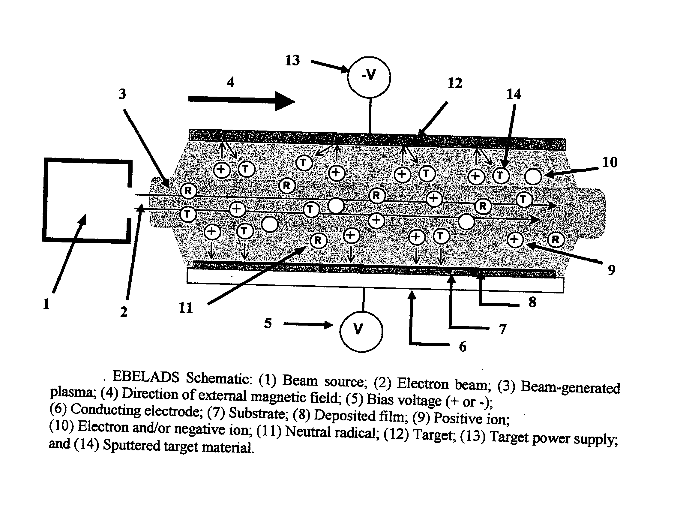
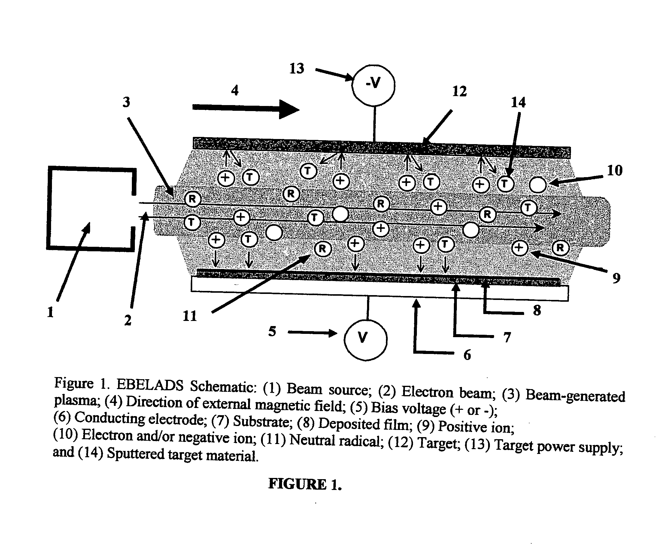
[0014] EBELADS is similar to LAPPS in concept and is illustrated in FIGS. 1. and 2. Specifically, EBELADS uses a magnetically confined, sheet electron beam to ionize and dissociate a background gas. The electron beam energy is nominally a few kiloelectron volts (keV) or less with beam current densities ranging from 1 to 100 mA / cm2 over the cross-section of the beam. The beam width is variable and can exceed a meter. The thickness is up to a few centimeters and is maintained over the beam length by an axial magnetic field that exceeds 100 Gauss. The length of the plasma sheet is determined by the range of the electron beam, and scales with the beam energy and gas pressure. The range is usually maintained at several times the system length to ensure uniformity in plasma production. The gas pressure typically lies between 10 and 100 mTorr. For the parameters outlined, the beam range is greater than 1 m and the plasma densities are as high as ˜1012 cm−3. Thus, the EBELADS system is capa...


PUM

PropertyMeasurementUnit
areasaaaaaaaaaa
thicknessaaaaaaaaaa
current densitiesaaaaaaaaaa

Abstract

This invention provides a means to deposit thin films and coatings on a substrate using an electron beam generated plasma. The plasma can be used as an ion source in sputter applications, where the ions are used to liberate material from a target surface which can then condense on a substrate to form the film or coating. Alternatively, the plasma may be combined with existing deposition sources including those based on sputter or evaporation techniques. In either configuration, the plasma serves as a source of ion and radical species at the growing film surface in reactive deposition processes. The electron beam large area deposition system (EBELADS) is a new approach to the production of thin films or coatings up to and including several square meters.

Description

BACKGROUND OF THE INVENTION [0001] 1. Field of the Invention [0002] This invention provides a means to produce large-area thin films and coatings. Thin films and coatings have applications in manufacturing, optics, and the semiconductor industries. Hard coatings can be used in tool manufacturing or for materials subject to high friction environments while corrosion resistant coatings can extend the lifetime of materials exposed to harsh chemical environments. Thin films can selectively increase or decrease the optical transmission properties of glass. In the semiconductor industry, thin films can be employed as a diffusion barrier between incompatible materials used in integrated circuit production. [0003] This invention utilizes an electron beam-produced plasma capable of generating ion and radical fluxes over large areas. The system can be configured as a large-area sputter source where the plasma ions are used to sputter (or remove) material from a target. This material then cond...

Claims


Application Information

Patent Timeline
Patent Type & Authority Applications(United States)
IPC IPC(8): C23C14/32C23C14/34H01L
CPCC23C14/3478
Inventor WALTON, SCOTT G.LEONHARDT, DARRINMEGER, ROBERT A.FERNSLER, RICHARDMURATORE, CHRISTORPHER
Owner THE UNITED STATES OF AMERICA AS REPRESENTED BY THE SECRETARY OF THE NAVY
Learn More