
Memory cell signal window testing apparatus

a technology of memory cell and signal window, which is applied in the direction of testing circuits, resistance/reactance/impedence, instruments, etc., can solve the problems of dramatic increase in failcount, dramatic decrease in yield, and the highest probability of failure of signal window higher than the tested window but lower than the main distribution during the lifetime of the chip

Inactive Publication Date: 2005-02-10
POLARIS INNOVATIONS
View PDF6 Cites 1 Cited by
  • Summary
  • Abstract
  • Description
  • Claims
  • Application Information

AI Technical Summary

Benefits of technology

[0008] The test mode of the present invention provides testing of FeRAM memory for a required signal window for each individual cell even with high parallel testing and with failure compression. Weak cells in FeRAM memories can be identified and repaired with minimum product yield loss.

Problems solved by technology

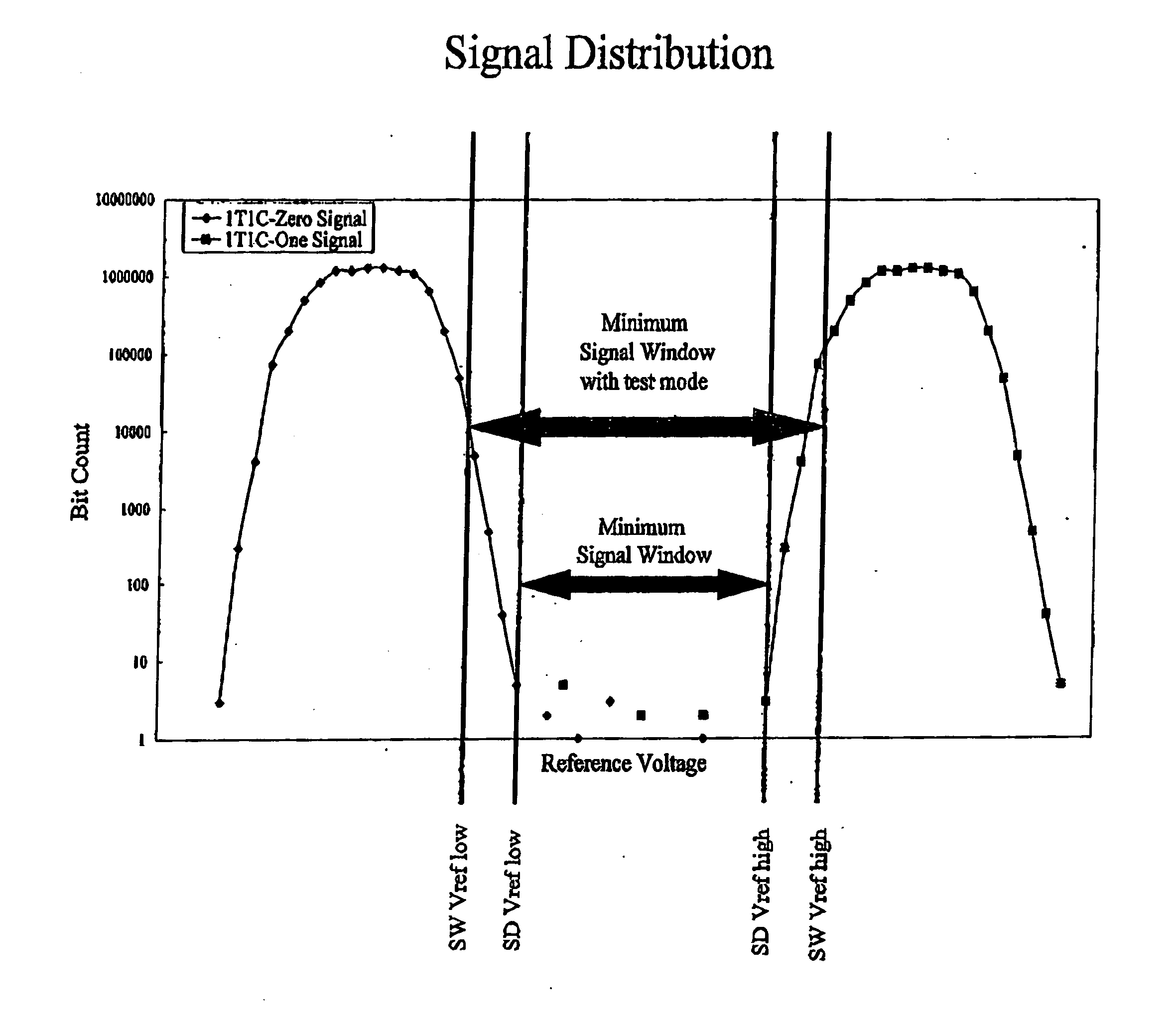
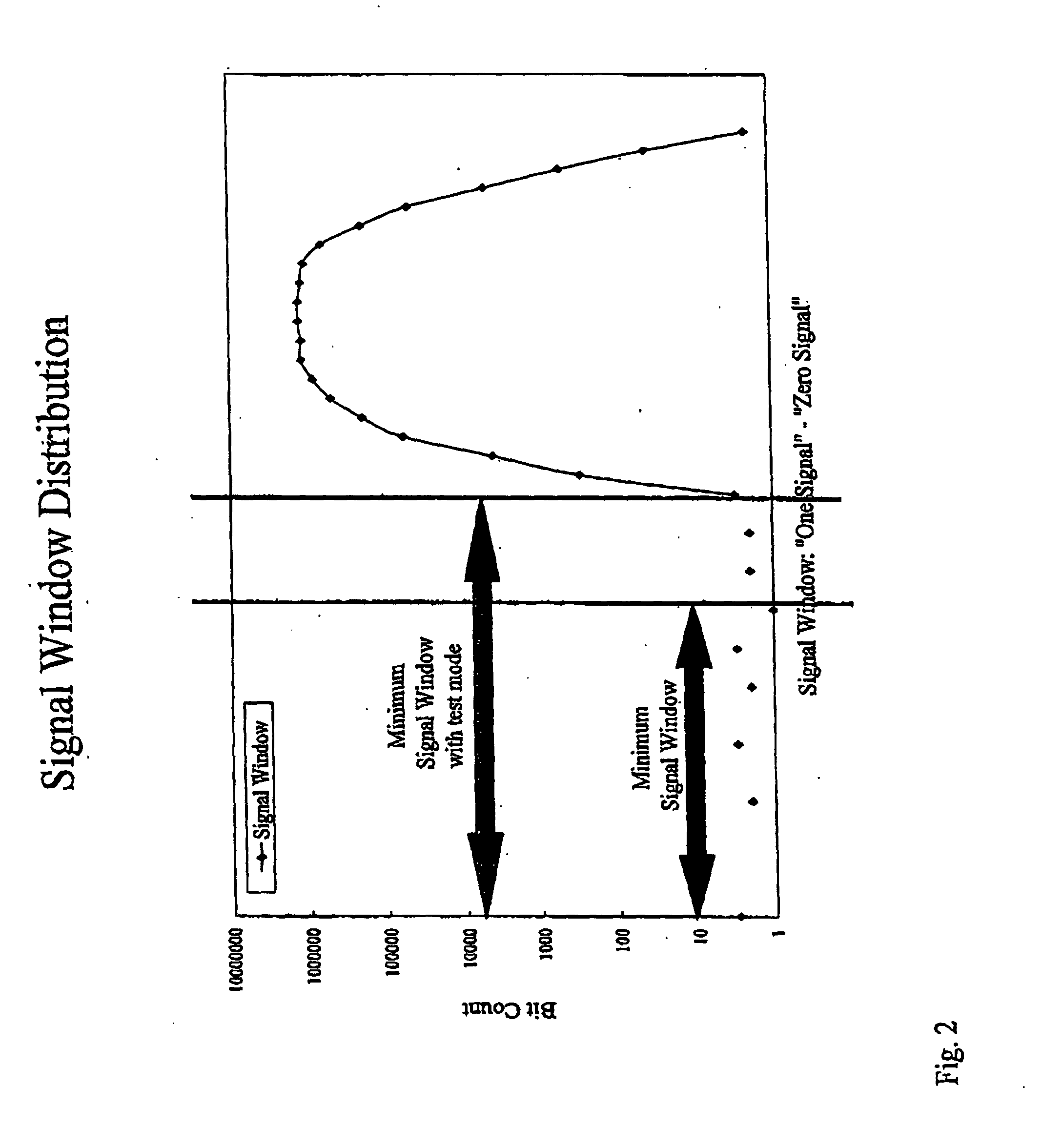
The cells with a signal window higher than the tested window but lower than the main distribution are most likely to fail during the lifetime of the chip.
But this method would lead to a dramatic increase in failcount and thus to a dramatic decrease in yield because even cells having a very good signal window would fail if one of their signals is at the wrong position in the distribution.
In high parallel testing of memory chips the failures are usually compress d to the smallest redundancy and therefore the information about which cell of a certain group of cells was failing the test is lost.
Due to this compression, it is not possible to test for single cells which are failing both test 1 AND test 2.
This criteria leads, however, to a certain yield loss, and in the worst case to chips which are sorted out even though they could have been repaired and used.

Method used


Image

  • Memory cell signal window testing apparatus
  • Memory cell signal window testing apparatus
  • Memory cell signal window testing apparatus

Examples


Embodiment Construction

[0015] A memory cell signal window testing apparatus 101 and method for testing the signal window of a memory are described with respect to FIGS. 3 and 4. The apparatus 101 can be on a memory chip as a test mode. At step 401 a BIST (Built In Self Test) controller 103 is enabled in response to receiving a signal input into a BIST Enable input 105.

[0016] At step 403 the BIST controller 103 sends a signal through a Vref Control (voltage reference control) input 111 to set a Vref Generator (reference voltage generator) 113 to output a SW Vref_low signal (signal window low reference volage signal) through the Vref output 115. The Vref is supplied to an array of memory cells 117 being tested.

[0017] At step 405 the BIST controller 103 sets the storage positions of a first storage register 109 to “0” (zero). The first storage register 109 can store 16 bits, for example.

[0018] At step 407 the “0” data in the first storage register 109 is written through an I / O (Input Output) control 131 t...


PUM


Abstract

A memory cell signal window testing apparatus 101 and method for testing the signal window of a memory are disclosed. First data is written to a memory cell during a write cycle. A low cell signal is read from the memory cell during a first read cycle. A comparison is made between the low signal and a low reference signal. The result of the comparison is stored in a first storage register. Second data is then written to the memory cell during a write cycle. A high cell signal is read from the memory cell during a second read cycle. A comparison is made between the high cell signal and a high reference signal. The result of the comparison is stored in a second storage register. The results in the first and second storage registers are compared and an output is provided indicating that the memory cell has failed the test if the comparison shows that both the low cell signal is higher than the low reference signal and the high cell signal is lower than the high reference signal.

Description

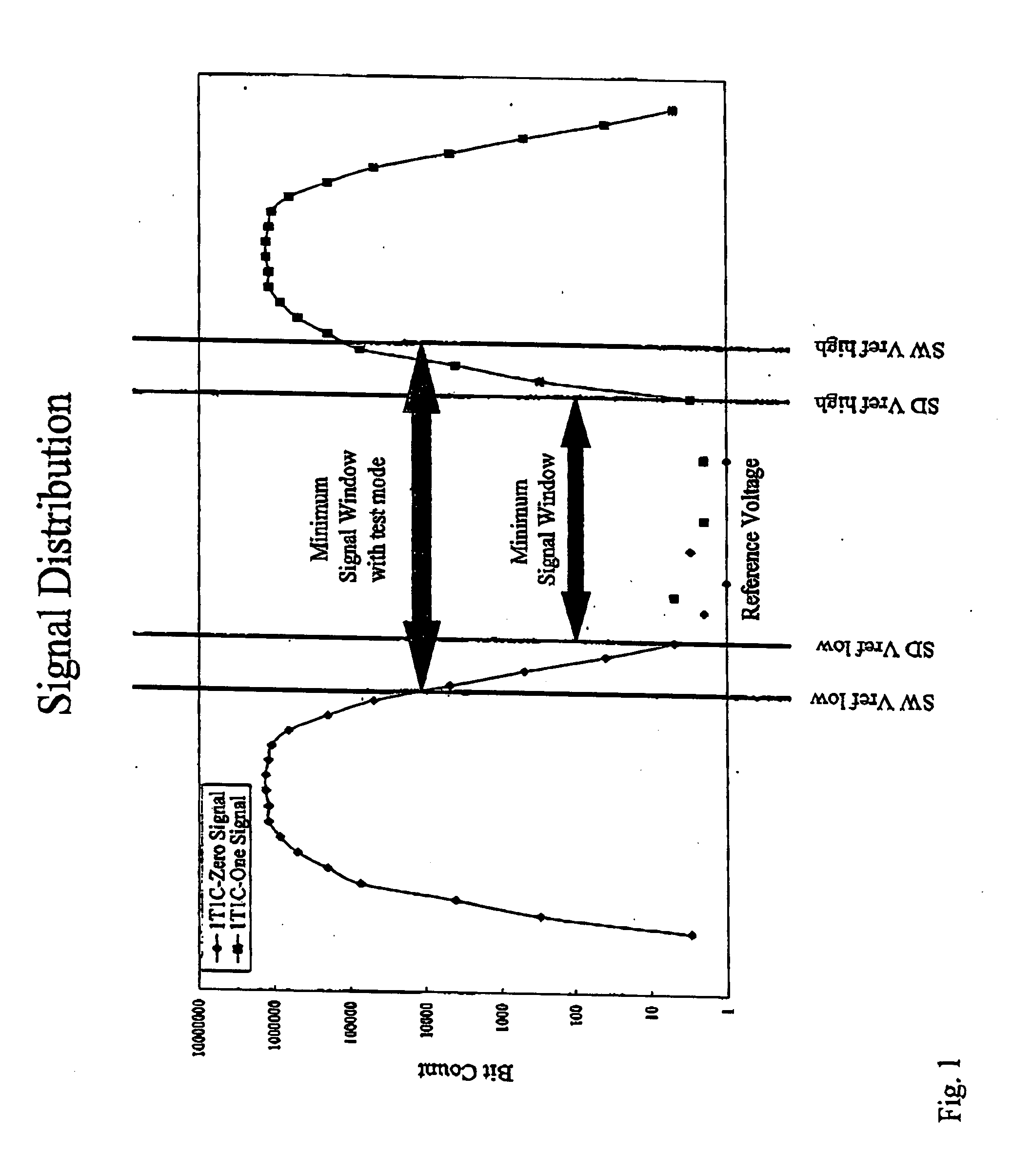
FIELD OF THE INVENTION [0001] The present invention relates to the testing of the signal window of memory cells. BACKGROUND OF THE INVENTION [0002] The signal window for a 1T1C FeRAM memory cell is tested using a low reference voltage (Signal Distribution reference voltage low—“SD Vref low”) and a high reference voltage (Signal Distribution reference voltage high—“SD Vref high”) and running some write / read patterns. FIG. 1 shows a signal distribution of an FeRAM memory chip and some typical low / high reference voltages for testing (SD Vref high / low). The signal window of an FeRAM memory cell is the difference of the high signal and the low signal of the cell. The minimum signal window for each cell which can be guaranteed by this prior-art test method is the difference between “SD Vref high” and “SD Vref low”. [0003] As shown in FIG. 2, the signal window distribution can show a main distribution which is much higher than the tested minimum signal window. The cells with a signal windo...

Claims


Application Information

Patent Timeline
IPC IPC(8): G06F19/00G11C11/22G11C11/4197G11C16/34G11C29/00G11C29/50
CPCG11C11/22G11C2029/5004G11C29/50
Inventor REHM, NORBERTJOACHIM, HANS-OLIVERJACOB, MICHAELWOHLFAHRT, JOERG
Owner POLARIS INNOVATIONS
Learn More