Integrated circuit structure and a design method thereof

Active Publication Date: 2005-02-03
ALICORP
View PDF13 Cites 6 Cited by
  • Summary
  • Abstract
  • Description
  • Claims
  • Application Information

AI Technical Summary

Benefits of technology

[0009] The main object of the present invention is to provide an integrated circuit structure and a design method thereof, in which the modifications are minimized when the circuit layout needs to be modified.
[0010] The secondary object of the present invention is to provide an integrated circuit structure and a design method thereof, by which the cost and time of research can be reduced.

Problems solved by technology

However, the expense of modification for taped out product is very amazing.
Since consumers require more and more functions, designed circuit becomes larger and larger and frequently contains millions of circuit elements.
Thus, the circuit elements are not probably accomplished one by one manually.
Besides, since elements of an integrated circuit are very numerous and their connection lines are further complicated, the elements cannot be connected one by one manually and usually are done in accordance with layout algorithm by a design software.
And, the expense of foundry is based on the number of changed masks.
It is a very astonishing cost.
Further, it takes time to re-design layout and re-produce connection line masks.

Method used


Image

  • Integrated circuit structure and a design method thereof
  • Integrated circuit structure and a design method thereof
  • Integrated circuit structure and a design method thereof

Examples


Embodiment Construction

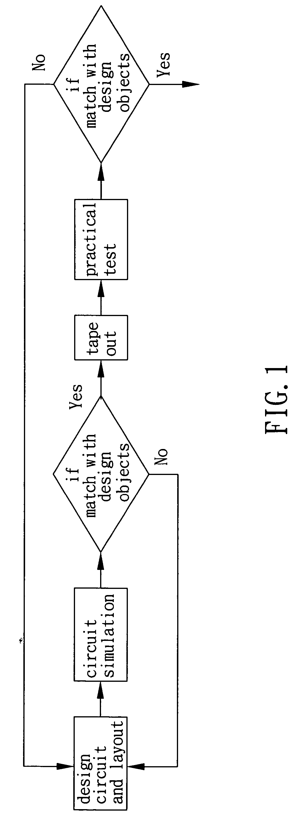
[0023] For your esteemed examiners to further recognize and understand the characteristics, objects, and functions of the invention, preferable embodiments cooperating with corresponding drawings are presented in detail thereinafter.

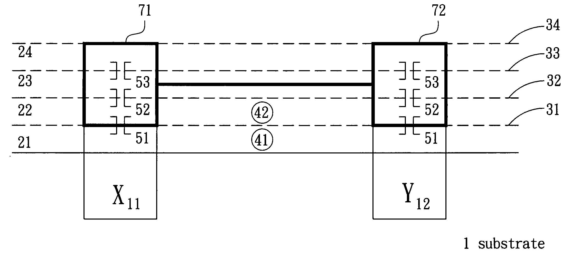
[0024] The spirit of the invention lies in prearranging a “circuit passageway” at each circuit element terminal in circuit simulation stage such that the same metal layer can be used to the best possibility when the design of circuit connections needs to be modified and thus the object of minimizing the number of modified masks can be achieved.

[0025] Please refer to FIG. 3, which is a schematic figure of integrated circuit modification of the invention. The invention provides an integrated circuit (IC) structure, comprising: [0026] a substrate 1, in which circuit elements, such as FET and CMOS formed by semiconductor processes, of an integrated circuit are placed, usually including pluralities of circuit elements; [0027] m metal layers, which are dispo...


PUM


Abstract

The present invention discloses an integrated circuit structure and a design method thereof, in which a circuit passageway is arranged at each circuit element terminal in circuit design stage. The arranged circuit passageway does not only increase layout flexibility in circuit simulation stage but also simplify layout difficulty when the circuit layout needs to be modified after taping out stage. Also, the circuit passageway can minimize modified metal layers, i.e. the number of modified masks is minimized. Because the expense of fab is based on the utilized layers and number of masks instead of designs of masks, the present invention will not increase the expense in taping out stage and can save the cost of research and development when modifications are required.

Description

BACKGROUND OF THE INVENTION [0001] (a) Field of the Invention [0002] The present invention relates to an integrated circuit structure and a layout design method thereof, and more particularly to an integrated circuit structure and a layout design method thereof which prearrange circuit passageways for reducing extent of modifying at future stage. [0003] (b) Description of the Prior Arts [0004] Along with the development of technologies, people further require features of communication products such as mobile phone or mobile products such as PDA to be lighter, thinner, shorter, and smaller so that applications of those integrated circuits (IC) satisfy with the above requirements are becoming broader and broader. Integrated circuit utilizes a way for three-dimensionizing a circuit to reduce the area used and can be frequently found in various applications. [0005] Please refer to FIG. 1, which is a design flow chart of an integrated circuit. Just like software design, even if source co...

Claims


Application Information

Patent Timeline
IPC IPC(8): H01L23/522H01L27/118H03K19/00
CPCH01L27/118H01L23/522H01L2924/0002H01L2924/00
Inventor KAN, TSANG-CHICHEN, WEN-LINGLIU, MIN-CHIH
Owner ALICORP
Why Eureka
Try Eureka