Method for manufacturing optical waveguide, optical waveguide device, electro-optical apparatus and electronic apparatus

Inactive Publication Date: 2005-01-27
SEIKO EPSON CORP
View PDF7 Cites 13 Cited by
  • Summary
  • Abstract
  • Description
  • Claims
  • Application Information

AI Technical Summary

Benefits of technology

[0012] According to this aspect of the present invention as defined above, when manufacturing an optical waveguide upon a substrate by utilizing an optical waveguide material (a material for manufacturing the optical waveguide) which is in its liquid form, and the like, before spreading the optical waveguide material upon the substrate, a liquid-repellent region is formed upon the substrate. Here, the liquid-repellent region is a region in which the optical waveguide material cannot easily be formed, while the optical waveguide material can easily be formed in the regions other than the liquid-repellent region. Thus, according to this aspect of the present invention, by forming the liquid-repellent region so as to surround the optical waveguide formation region upon the substrate, upon which the optical waveguide is to be formed, and by thereafter loading the optical waveguide material within this optical waveguide formation region, and the like, it is possible to control the shape of the optical waveguide (its line width, the shape in which it curves, its cross sectional shape, and so on) easily and moreover at high accuracy. Furthermore, according to this aspect of the present invention, even when the optical waveguide materials have been spread upon the entire surface of the substrate, the optical waveguide material which has been spread over the liquid-repellent region experiences an action to impel it out from that region, accordingly it is possible to manufacture an extremely accurate optical waveguide in a very simple manner.
[0069] Furthermore, according to the present invention as defined above, by, for example, applying the above described optical waveguide device to a display device, it is possible to provide a cheap electronic device which can display an image of high quality at high speed.

Problems solved by technology

However, a bottleneck has arisen with regard to the processing speed of computers, due to the fact that a bound has almost been reached in the signal transmission speed over the bus which connects the CPU and the peripheral devices such as storage devices.
However, if an optical fiber is taken advantage of as a light transmission device, the task of connecting together the various optical components such as a light emitting element and a light reception element and so on becomes complicated, and the problem arises that, along with the manufacture of the device becoming very costly and taking a long time, it becomes difficult to make this light transmission device compact.
However, a light transmission device which utilizes an optical waveguide has not yet been implemented, for which its miniaturization and facilitation of construction have progressed as far as making it conceivably possible to use this light transmission device in a flat display device or a computer or the like.
In particular, the implementation of techniques for controlling the formation of such an optical waveguide, including its line width, easily and moreover at high accuracy have been inadequate.

Method used


Image

  • Method for manufacturing optical waveguide, optical waveguide device, electro-optical apparatus and electronic apparatus
  • Method for manufacturing optical waveguide, optical waveguide device, electro-optical apparatus and electronic apparatus
  • Method for manufacturing optical waveguide, optical waveguide device, electro-optical apparatus and electronic apparatus

Examples


Embodiment Construction

[0092] In the following, preferred embodiments of the method for manufacturing an optical waveguide according to the present invention, and of the optical waveguide device according to the present invention, will be explained with reference to the drawings.

[0093] (Structural Example)

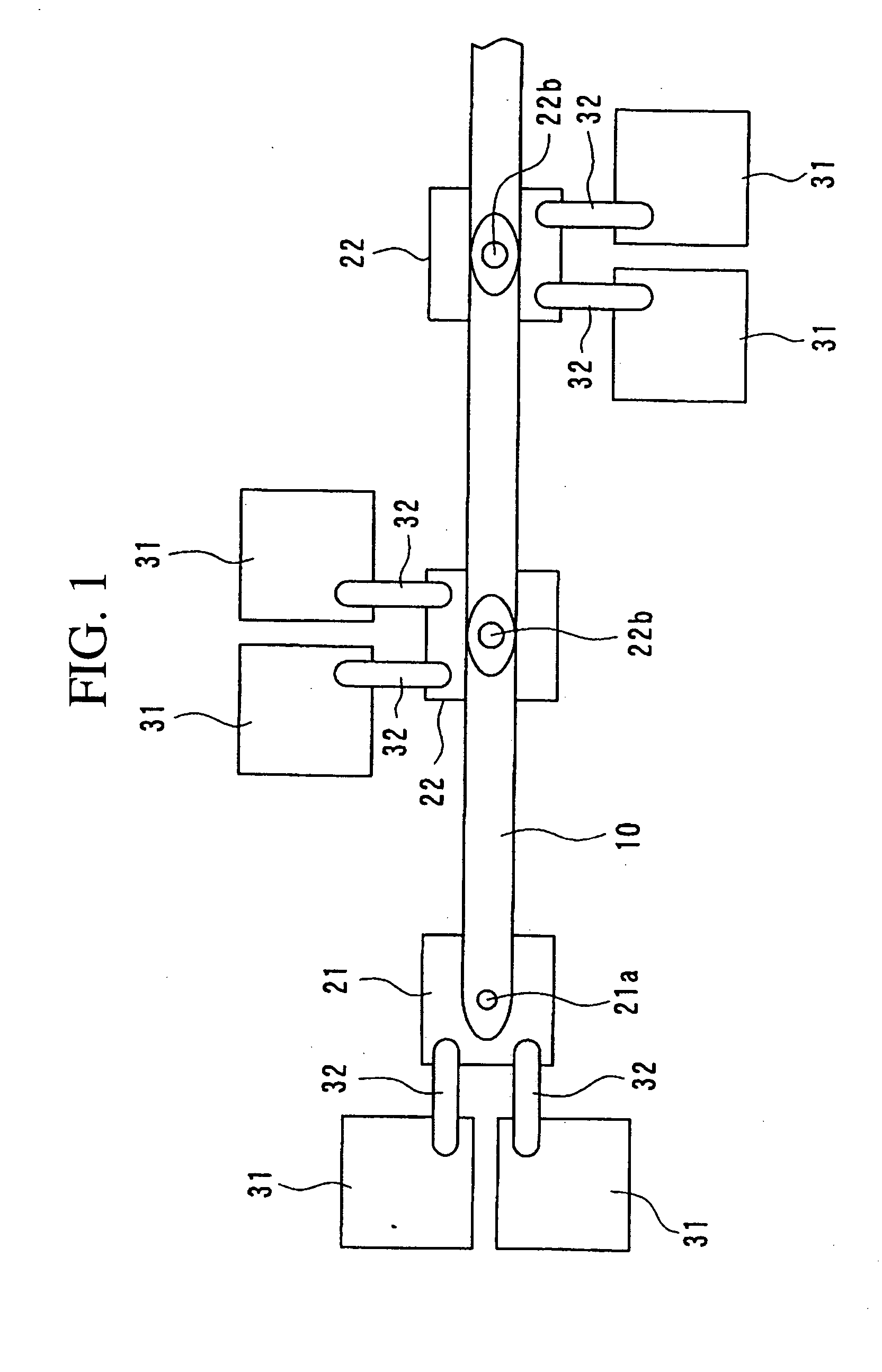
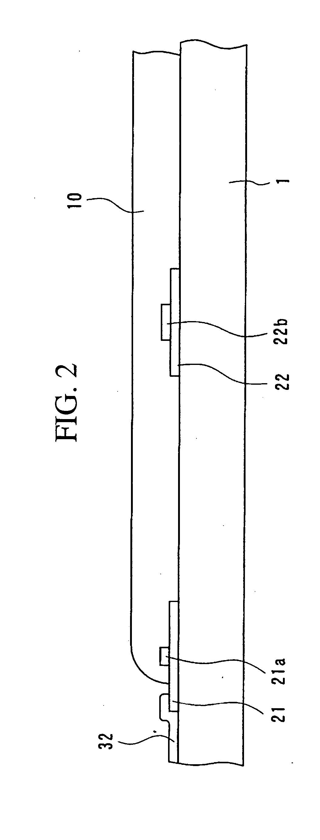
[0094] First, an example of the structure of an optical waveguide device according to a preferred embodiment of the present invention will be explained with reference to FIGS. 1 and 2. FIG. 1 is a plan view showing such an optical waveguide device according to a preferred embodiment of the present invention. In addition, FIG. 2 is a partial sectional view of the optical waveguide device shown in FIG. 1.

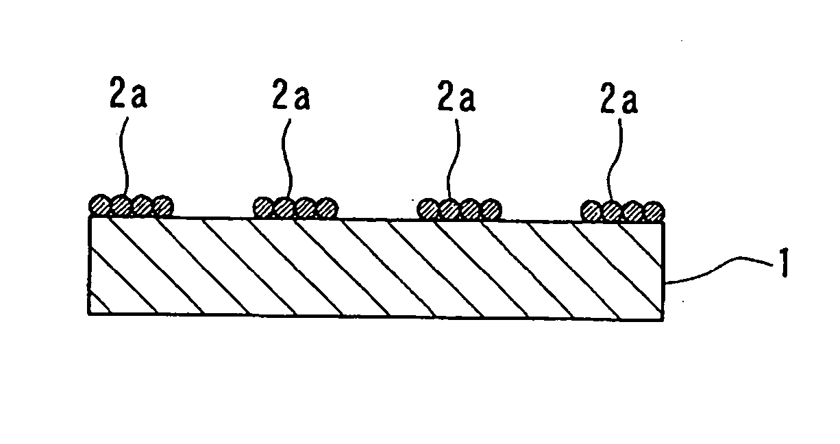
[0095] This optical waveguide device includes an optical waveguide 10 formed upon the surface of a substrate 1 or the like, micro tile shaped elements 21 and 22 which are adhered to the surface of the substrate 1 or the like, and bonding pads 31 which are formed upon the surface of the substrate 1 or th...


PUM

PropertyMeasurementUnit
Wavelengthaaaaaaaaaa
Temperatureaaaaaaaaaa
Shapeaaaaaaaaaa

Abstract

A method for manufacturing an optical waveguide includes the steps of forming a liquid-repellent region upon a substrate, and forming the optical waveguide in a region upon the substrate other than the liquid-repellent region.

Description

BACKGROUND OF THE INVENTION [0001] 1. Field of the Invention [0002] The present invention relates to a method for manufacturing an optical waveguide, an optical waveguide device, an electro-optical apparatus and an electronic apparatus. [0003] Priority is claimed on Japanese Patent Application No. 2003-169816, filed Jun. 13, 2003, the content of which is incorporated herein by reference. [0004] 2. Description of Related Art [0005] In recent years, electroluminescent panels (ELPs), plasma display panels (PDPs), and liquid crystal display devices (LCDs) and the like have been utilized as planar display devices. In addition, as is shown, for example, in Japanese Unexamined Patent Application, First Publication No. 5-100246, techniques utilized for optical signal transmission has been investigated, in order to eliminate signal delay and the like which accompanies increase in the size and increase in the display capability of these flat display devices. [0006] Furthermore, in recent year...

Claims


Application Information

Patent Timeline
IPC IPC(8): C03C17/02C03C17/32G02B6/12G02B6/122G02B6/13G02B6/138G02B6/43H01L21/60
CPCB82Y10/00H01L2224/24051C03C17/02C03C17/32C03C2218/113C03C2218/114C03C2218/34G02B6/13G02B6/138G02B6/43G02B2006/12166H01L24/24H01L24/82H01L2221/68354H01L2221/68368H01L2224/24226H01L2224/76155H01L2224/92244H01L2924/01013H01L2924/01046H01L2924/01079H01L2924/01082H01L2924/09701H01L2924/14H01L2924/30105H01L2924/01005H01L2924/01006H01L2924/01033H01L2924/12041H01L2224/82102B82Y30/00H01L2924/12042H01L2924/12043H01L2924/12044H01L2924/00
Inventor TAKAKUWA, ATSUSHIKONDO, TAKAYUKI
Owner SEIKO EPSON CORP
Why Eureka
Try Eureka