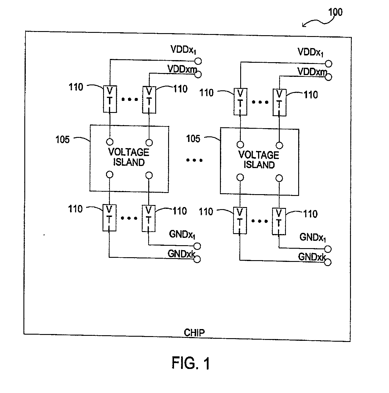
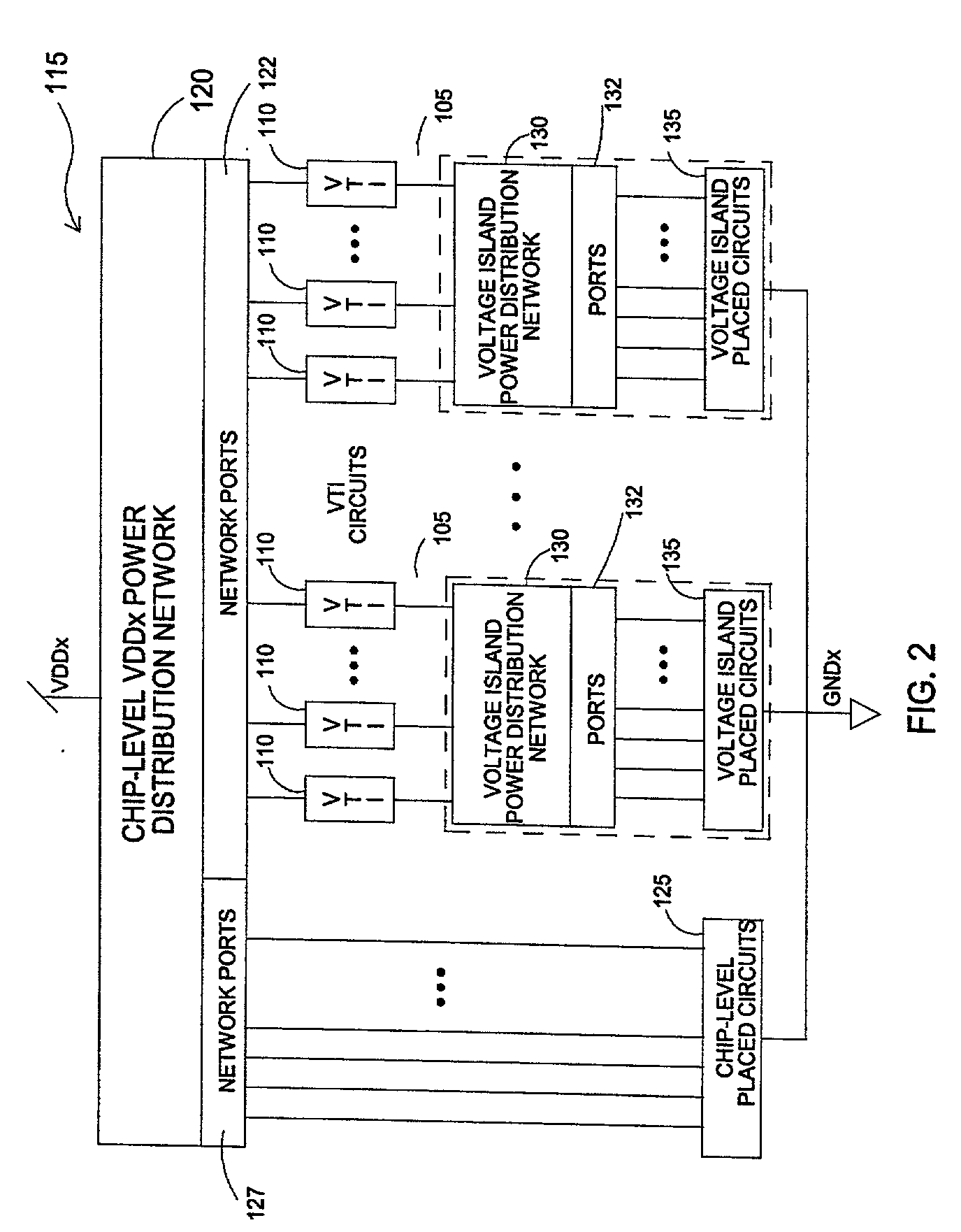
0013] A first aspect of the present invention is a method of analyzing the power distribution in a chip containing one or more voltage islands, each voltage island having a power distribution network connected to a chip-level power distribution network by one or more voltage translation interface circuits comprising: analyzing the voltage-island power distribution networks independently of the chip-level power distribution network to obtain voltage translation interface circuit currents; using the voltage translation interface circuit currents as input to a model of the chip-level power distribution network to obtain voltage translation interface circuit input voltages; and calculating voltage translation interface circuit output voltages based on the voltage translation interface circuit input voltages, the voltage translation interface circuit currents, and current-voltage characteristics of the voltage translation interface circuits.
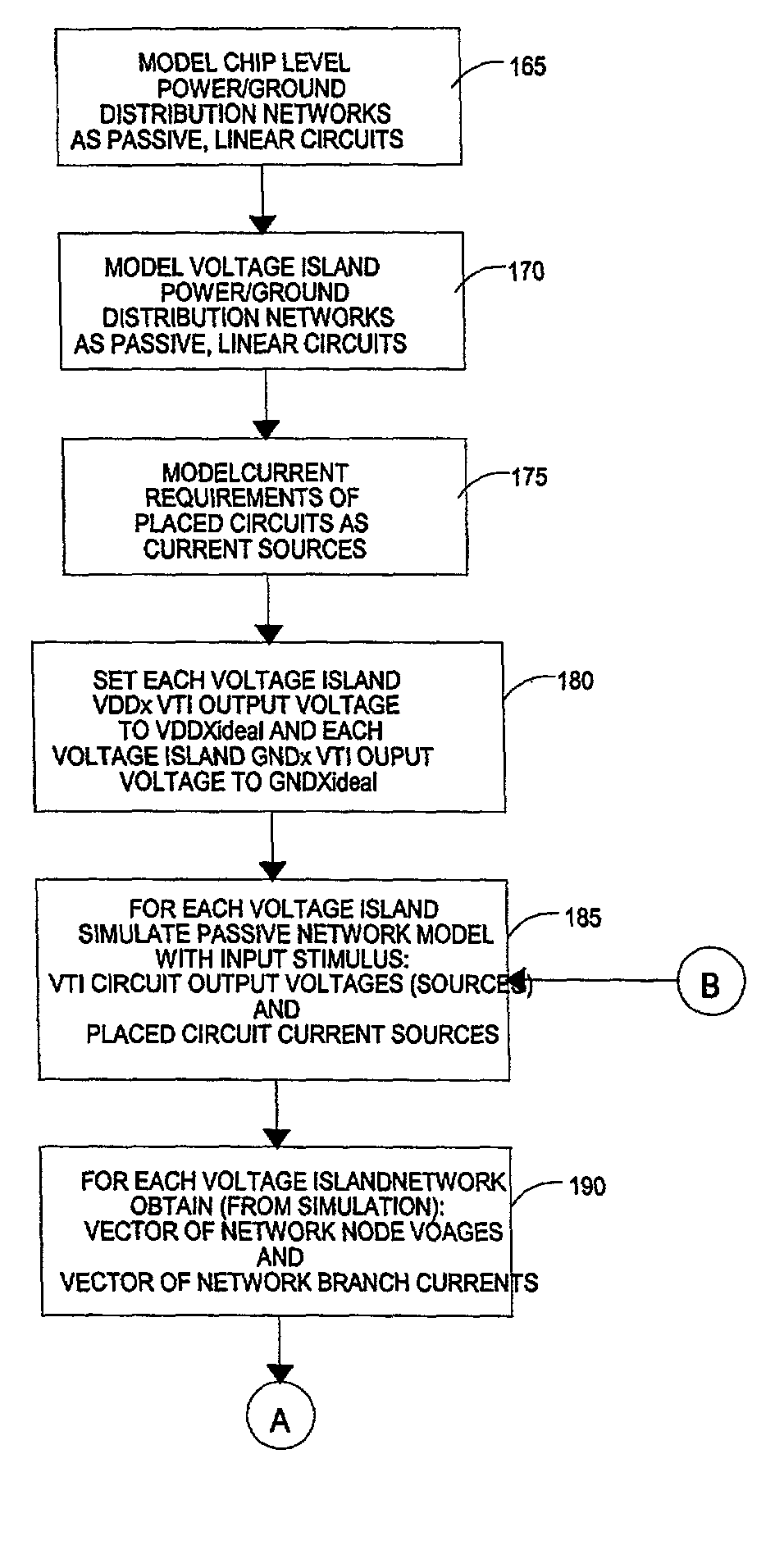
0014] A second aspect of the present invention is method of analyzing power distribution in a chip containing one or more voltage islands, each voltage island having a power distribution network connected to a chip-level power distribution network by one or more voltage translation interface circuits comprising: (a) creating a chip-level power distribution network model connected to chip-level placed circuits modeled as current sources; (b) independently creating a voltage-island power distribution network model connected between voltage translation interface circuit outputs and voltage-island placed circuits modeled as current sources; (c) obtaining voltage translation interface circuit currents by: (i) in a first iteration, using the ideal value of an external voltage source as the value of the voltage translation interface circuit output voltages; (ii) in subsequent iterations using the most recently computed values for the voltage translation interface circuit output voltages; and (iii) simulating the voltage-island power distribution with its corresponding external voltage sources and the most recently obtained values of the voltage translation interface circuit currents; (d) exciting the chip-level power distribution with the most recently obtained values of the voltage translation interface circuit currents; (e) obtaining, through simulation of the chip-level power distribution network, values for the voltage translation interface circuit input voltages and values for the chip-level placed circuit port voltages; (f) calculating updated values for the voltage translation interface circuit output voltages, based on the most recently obtained values for the voltage translation interface circuit input voltages, the currents through the voltage translation interface circuits, and the current-voltage characteristics of the voltage translation interface circuits; and (g) comparing the updated values to immediately previous values for the chip-level placed circuit port voltages, voltage translation interface circuit input voltages, and voltage translation circuit output voltages, and, if not converged to within a preset limit, repeating steps (c) through (g).
0015] A third aspect of the present invention is a program storage device readable by machine, tangibly embodying a program of instructions executable by the machine to perform method steps for analyzing power distribution in a chip containing one or more voltage islands, each voltage island having a power distribution network connected to a chip-level power distribution network by one or more voltage translation interface circuits, the method steps comprising: (a) creating a chip-level power distribution network model connected to chip-level placed circuits modeled as current sources; (b) independently creating a voltage-island power distribution network model connected between voltage translation interface circuit outputs and voltage-island placed circuits modeled as current sources; (c) obtaining voltage translation interface circuit currents by: (i) in a first iteration, using the ideal value of an external voltage source as the value of the voltage translation interface circuit output voltages; (ii) in subsequent iterations using the most recently computed values for the voltage translation interface circuit output voltages; and (iii) simulating the voltage-island power distribution with its corresponding external voltage sources and the most recently obtained values of the voltage translation interface circuit currents; (d) exciting the chip-level power distribution with the most recently obtained values of the voltage translation interface circuit currents; (e) obtaining, through simulation of the chip-level power distribution network, values for the voltage translation interface circuit input voltages and values for the chip-level placed circuit port voltages; (f) calculating updated values for the voltage translation interface circuit output voltages, based on the most recently obtained values for the voltage translation interface circuit input voltages, the currents through the voltage translation interface circuits, and the current-voltage characteristics of the voltage translation interface circuits; and (g) comparing the updated values to immediately previous values for the chip-level placed circuit port voltages, voltage translation interface circuit input voltages, and voltage translation circuit output voltages, and, if not converged to within a preset limit, repeating steps (c) through (g).
0016] A fourth aspect of the present invention is a computer system comprising a processor, an address / data bus coupled to the processor, and a computer-readable memory unit coupled to communicate with the processor, the memory unit containing instructions that when executed implement a method for analyzing power distribution in a chip containing one or more voltage islands, each voltage island having a power distribution network connected to a chip-level power distribution network by one or more voltage translation interface circuits, the method comprising the computer implemented steps of: (a) creating a chip-level power distribution network model connected to chip-level placed circuits modeled as current sources; (b) independently creating a voltage-island power distribution network model connected between voltage translation interface circuit outputs and voltage-island placed circuits modeled as current sources; (c) obtaining voltage translation interface circuit currents by: (i) in a first iteration, using the ideal value of an external voltage source as the value of the voltage translation interface circuit output voltages; (ii) in subsequent iterations using the most recently computed values for the voltage translation interface circuit output voltages; and (iii) simulating the voltage-island power distribution with its corresponding external voltage sources and the most recently obtained values of the voltage translation interface circuit currents; (d) exciting the chip-level power distribution with the most recently obtained values of the voltage translation interface circuit currents; (e) obtaining, through simulation of the chip-level power distribution network, values for the voltage translation interface circuit input voltages and values for the chip-level placed circuit port voltages; (f) calculating updated values for the voltage translation interface circuit output voltages, based on the most recently obtained values for the voltage translation interface circuit input voltages, the currents through the voltage translation interface circuits, and the current-voltage characteristics of the voltage translation interface circuits; and (g) comparing the updated values to immediately previous values for the chip-level placed circuit port voltages, voltage translation interface circuit input voltages, and voltage translation circuit output voltages, and, if not converged to within a preset limit, repeating steps (c) through (g).


