
Buried strap formation method for sub-150 nm best DRAM devices

a buried strap and dram technology, applied in the direction of semiconductor devices, basic electric elements, electrical equipment, etc., can solve the problems of poor control of the inability of the scheme to accurately control the depth, thickness and doping level and the inability to accurately control the diffusion length and resistivity of the buried strap

Inactive Publication Date: 2003-06-12
CHANG LIAO HLDG
View PDF0 Cites 21 Cited by
  • Summary
  • Abstract
  • Description
  • Claims
  • Application Information

AI Technical Summary

Problems solved by technology

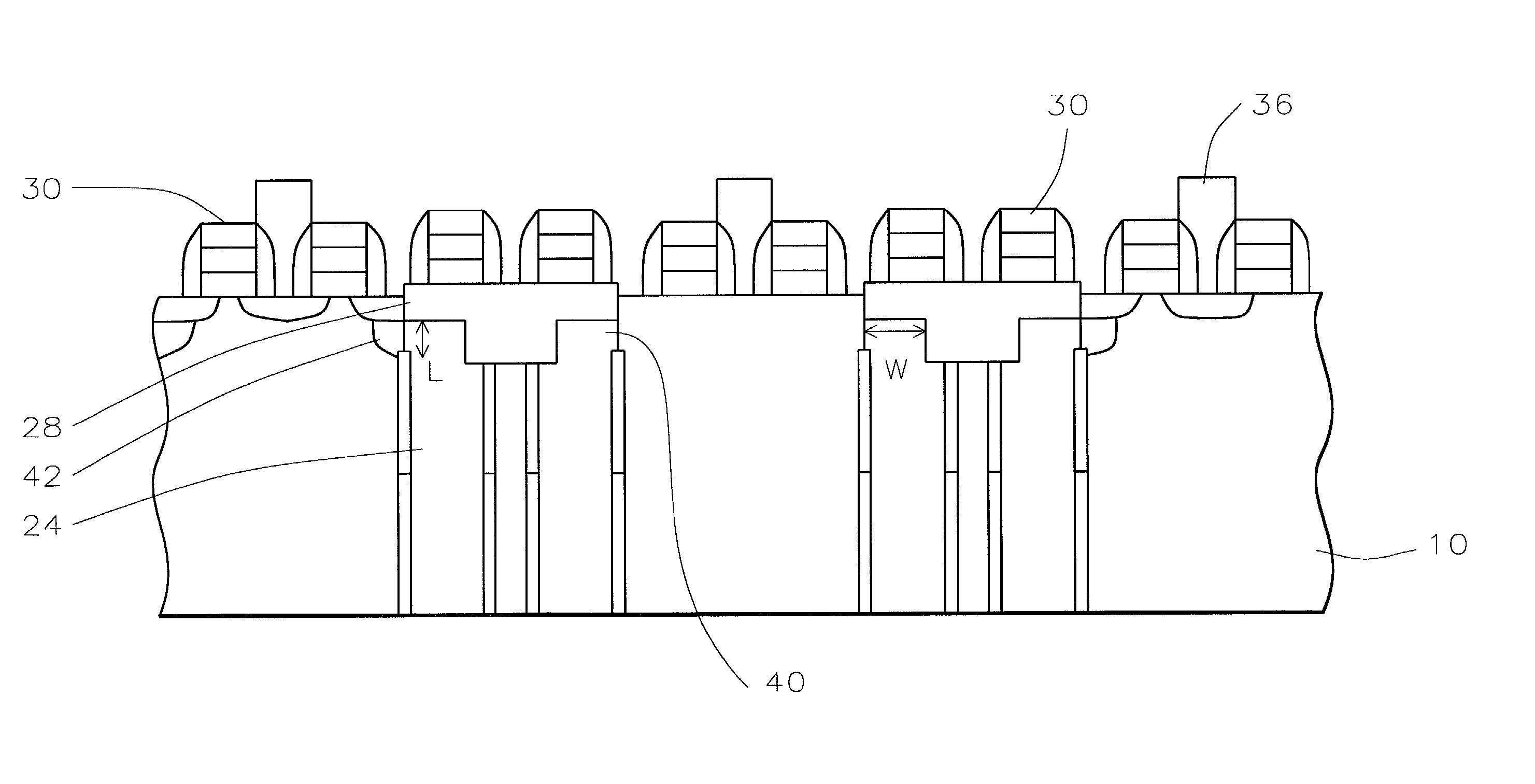
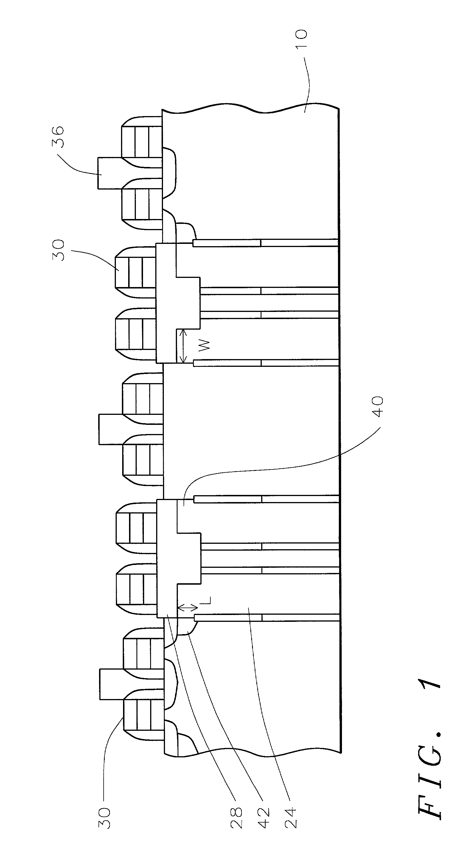
Therefore, control of diffusion length and resistivity of the buried strap are key issues for a healthy interconnect between array devices and capacitors.
However, this conventional scheme cannot accurately control the buried strap depth, thickness, and doping level because of the complex interactions of the recess 2, collar removal, and recess 3 steps.
Thus, the buried strap junction diffusion is poorly controlled.
A shallow etch results in over diffusion causing short channel effects while a deep etch results in an open circuit, cutting off the current path.
This limited controllability makes the BuriEd STrap (BEST) DRAM cell extendibility limited to a shorter generation.

Method used


Image

  • Buried strap formation method for sub-150 nm best DRAM devices
  • Buried strap formation method for sub-150 nm best DRAM devices
  • Buried strap formation method for sub-150 nm best DRAM devices

Examples


Embodiment Construction

process. U.S. Pat. No. 5,981,332 to Mandelman et al shows a BEST DRAM process.

[0008] Accordingly, it is a primary object of the present invention to provide an effective and very manufacturable method of BEST DRAM formation in the fabrication of integrated circuits.

[0009] It is a further object of the invention to provide a method of forming an improved buried strap in DRAM device fabrication.

[0010] Another object of the invention is to provide an improved buried strap formation method using a selective hemispherical grain (HSG) method in the fabrication of a DRAM integrated circuit device.

[0011] Yet another object of the invention is to provide an improved buried strap formation method using plasma doping in the fabrication of a DRAM integrated circuit device.

[0012] A further object of the invention is to provide an improved buried strap formation method having a ground rule of less than or equal to 0.25 .mu.m in the fabrication of a DRAM integrated circuit device.

[0013] A still fu...


PUM


Abstract

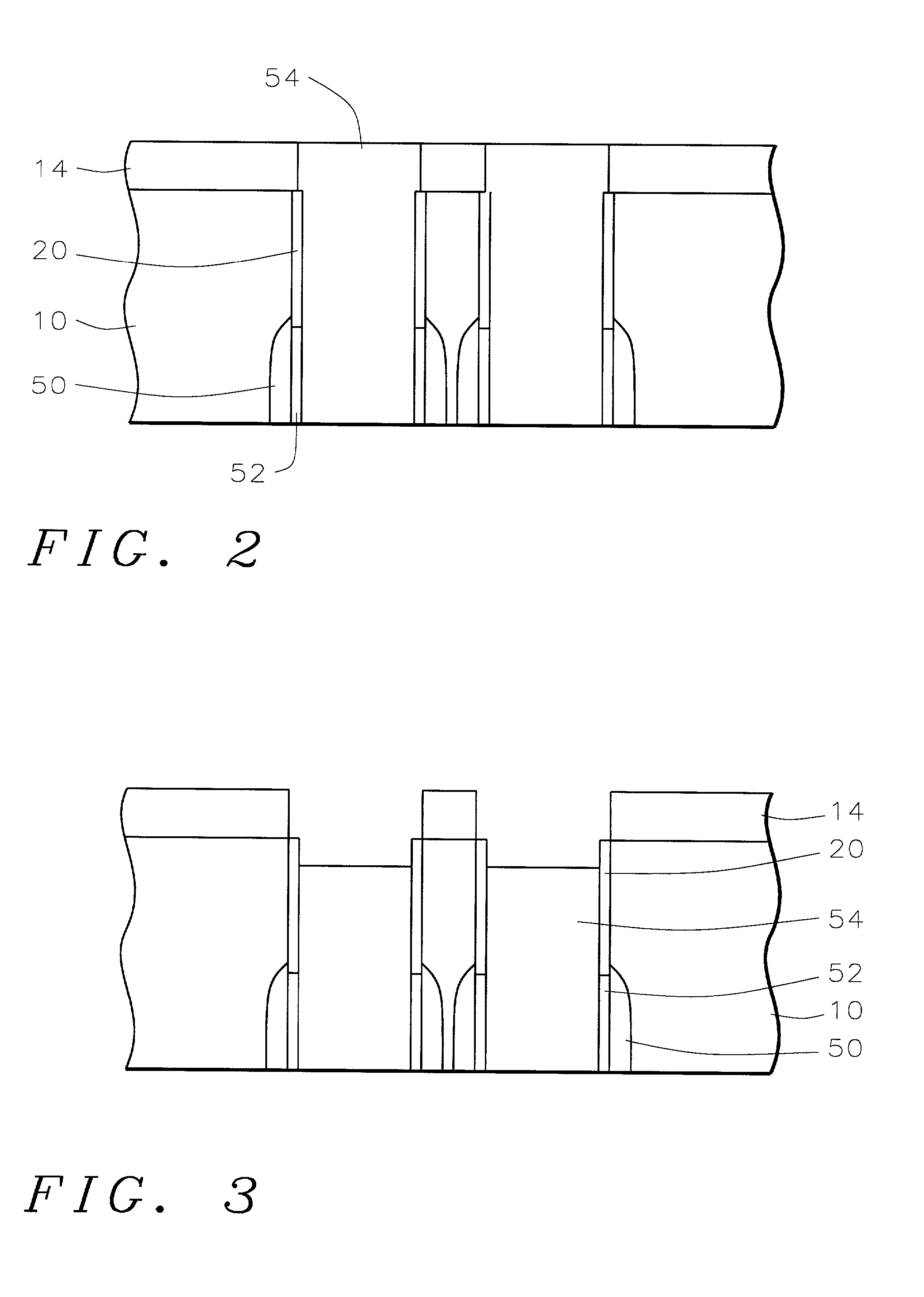
An improved buried strap method in the fabrication of a DRAM integrated circuit device is described. A deep trench is etched into a substrate. A collar is formed on an upper portion of the deep trench. A buried plate is formed by doping around a lower portion of the deep trench and a capacitor dielectric layer is formed within the deep trench. The deep trench is filled with a silicon layer wherein the silicon layer forms a deep trench capacitor and covers the collar. The silicon layer is recessed below a top surface of the substrate to leave a recess. A top portion of the collar is etched away to leave a collar divot. A hemispherical grain polysilicon layer is selectively deposited into the deep trench and filling the collar divot. The HSG layer is doped in-situ or by post plasma doping. The doped hemispherical grain polysilicon layer forms a buried strap in the fabrication of a deep trench DRAM integrated circuit device.

Description

[0001] (1) Field of the Invention[0002] The present invention relates to the fabrication of integrated circuit devices, and more particularly, to a method of fabricating an improved buried strap in deep trench DRAM devices in the fabrication of integrated circuits.[0003] (2) Description of the Prior Art[0004] In the fabrication of integrated circuit devices, a buried strap has been used in fabricating deep trench (DT)-based dynamic random access memory (DRAM) devices. The buried strap is a crucial part of the integration step connecting a storage node capacitor to an array switching transistor by forming a diffusion junction. Therefore, control of diffusion length and resistivity of the buried strap are key issues for a healthy interconnect between array devices and capacitors. The diffusion length and resistivity primarily depend upon buried strap width and thickness and thermal budget during post processes.[0005] In a conventional deep trench process, a deep trench is etched. A sa...

Claims


Application Information

Patent Timeline
Patent Type & Authority Applications(United States)
IPC IPC(8): H01L21/762H10B12/00
CPCH01L27/10867H01L21/76224H10B12/0385
Inventor LEE, BRIAN
Owner CHANG LIAO HLDG
Learn More