One-shot signal generating circuit

Inactive Publication Date: 2003-05-15
RENESAS ELECTRONICS CORP
View PDF0 Cites 2 Cited by
  • Summary
  • Abstract
  • Description
  • Claims
  • Application Information

AI Technical Summary

Benefits of technology

[0028] The present invention was conceived against this type of background, and its objective is to provide a one-shot signal generation circuit with which, by providing, for example, ring oscillators and a plurality of frequency division circuits connected in a cascade, adjustment of the pulse width and countermeasures against variation of the skew of the ATD signals becomes easy, so that it is capable of stably generating a one-shot signal.
[0038] By doing as described above, the present invention can utilize a structure in which the pulse width of the one-shot signal is adjusted not by separate delay circuits, but for example by a single delay circuit and frequency division circuit, and resets the frequency division circuits with the respective address transition detection signals. As a result, it is possible to determine the generation timing and termination timing of the one-shot signal according to a pulse of suitable timing even when the address transition detection signal has been divided into a plurality thereof. Furthermore, it is possible to bring the adjustment points for timing into a single point, so that it is possible to perform reduction of the chip area. Moreover, it is possible to attain the objects without utilizing a circuit with large fan out, since it is possible to obtain the required delay time by frequency dividing the outputs of short delay circuits.

Problems solved by technology

However, with the address transition detection circuits according to the background art, problems occur like the following due to the use of various types of delay circuit such as the delay circuit 170 for determining the pulse width of the ATD signal and the inverter gates 7 for timing adjustment and so on.
Accordingly, with this circuit system, there are the problems that the occupancy area upon the chip becomes large, and moreover the power consumption is increased by the activation of the large number of inverter gates of high drive power.
Accordingly, with this circuit system, it becomes easy for the delay time of the inverter gates which are connected in a cascade to suffer the influence of production deviations, and the problem arises that it becomes difficult to obtain an accurate delay time.
In this manner, according to the structure shown in FIG. 19, when the period of the address signal becomes short, the problem arises that the pulse width becomes narrow.
As has been explained above, according to the background art described above, since the pulse width of the one-shot signal is determined using a delay circuit, the pulse width of the one-shot signal easily suffers influences from variations in the delay time of the delay circuit, skew of the input signals, variations in the period of the input signals, short pulses occurring in the input signals, and the like, so that it is not possible to generate the one-shot signal stably.

Method used


Image

  • One-shot signal generating circuit
  • One-shot signal generating circuit
  • One-shot signal generating circuit

Examples


first embodiment

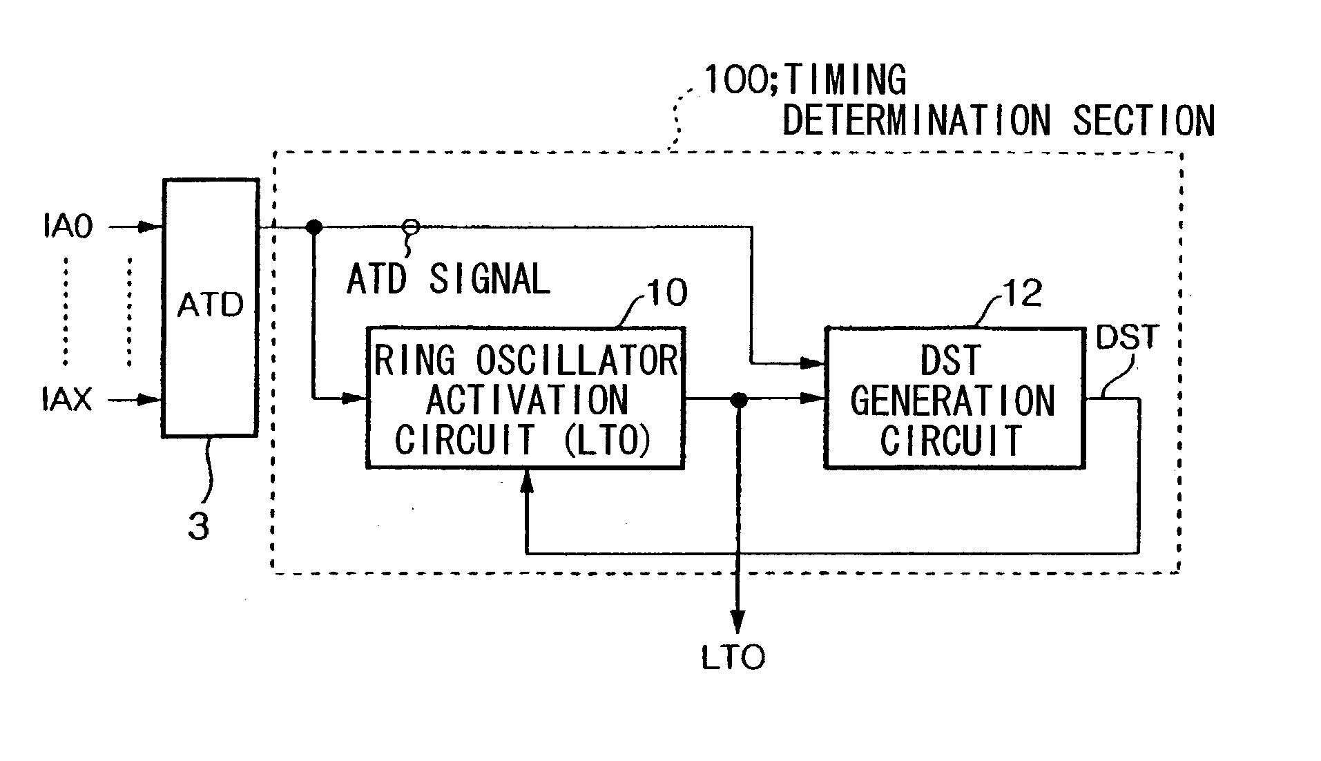
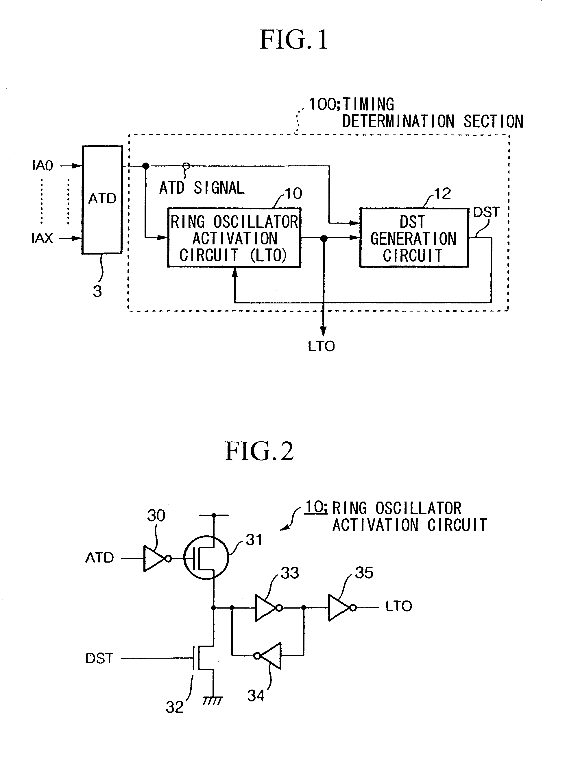
[0066] FIG. 1 shows the structure of a one-shot signal generation circuit according to the present invention. This one-shot signal generation circuit is used in an asynchronous memory, and it generates a one-shot signal LTO for determining an internal operational timing in response to a change in input signals such as address signals.

[0067] In this figure, the reference symbol 3 denotes an address transition detection circuit (ATD; Address Transition Detector) which detects transition of an address signal IA0-IAX (input signals) and generates an ATD signal (a pulse signal). In this first embodiment, the edge of the ATD signal has a more important meaning than its pulse width. In other words, the pulse width of the ATD signal which is generated by the address transition detection circuit 3 may be narrow provided that at least the arrival of its rising edge and its falling edge are significant, so that it will be sufficient for it to be set so that its edges arrive sharply.

[0068] The ...

second embodiment

[0092] In the following, the present invention will be explained.

[0093] The structure of the one-shot signal generation circuit according to this second embodiment of the present invention is shown in FIG. 6. With the first embodiment, it was arranged that the timing of the end edge of the one-shot signal was determined according to the final ATD signal in the skew period of the address signal; but, in this second embodiment, the timing of both the start edge and the end edge of the one-shot signal are determined by the single initial ATD signal in the same skew period.

[0094] In FIG. 6, the reference symbol 3 denotes an address transition detection circuit (ATD), and it is the same as the one according to the first embodiment. The reference symbol 110 denotes a timing determination section, and this, along with functioning as a circuit section for generating a one-shot signal LTPG, also is a timing determination section which determines the timing of the edge of this one-shot signal...

third embodiment

[0108] In the following, the present invention will be explained.

[0109] In this third embodiment, a one-shot signal generation circuit will be explained which generates a one-shot signal as a latch signal which is used for latching an external address, by the timing determination section 100 according to the first embodiment and the timing determination section 110 according to the second embodiment being employed together.

[0110] FIG. 10 is a block diagram showing the structure of the one-shot signal generation circuit according to this third embodiment. Moreover, a circuit diagram of an LC generation circuit 14 and an example of its operational waveform are respectively shown in FIGS. 11A and 11B. In FIG. 10, the same reference symbols are assigned to structural elements which are common to the first and second embodiments.

[0111] The ring oscillator activation circuit (LT0) 10, the ring oscillator activation circuit (LTPG) 11, the DST generation circuit 12, and the PG generation ci...


PUM


Abstract

A one-shot signal generation circuit is provided which makes it easy to adjust pulse width and to deal with variation of skew of an ATD signal, and can reduce chip area. A timing determination section (100) is reset by an edge of a first detected signal among a plurality of address transition detection signals (ATD signals) which have arrived within the skew period of an address signal, measures a first predetermined time by taking an edge of a second detected signal as start instant, and outputs a signal DST which reflects the result of this measurement. A timing determination section (110) measures a second predetermined time by taking an edge of the first detected signal as start instant, and outputs a signal PG which reflects the result of this measurement. An LC generation circuit (14) outputs a one-shot signal (LC) whose start instant is determined by the signal PG and whose end instant is determined by the signal DST.

Description

[0001] This invention relates to a one-shot signal generation circuit which generates a one-shot signal for determining the internal operational timing of an asynchronous memory.[0002] As a conventional asynchronous memory, there has been a memory which operates by generating a one-shot signal internally when an external address has changed. As a one-shot signal generation circuit for generating this one-shot signal, generally a circuit as shown in FIG. 19 is employed. The one-shot signal generation circuit shown in this figure detects change (transition) of address signals A0-AX which are its input signals, generates a plurality of address transition detection signals (hereinafter termed ATD signals) in pulse form, and combines these ATD signals into a single one-shot signal. Various internal signals for providing timing for internal operations, such as latch signals for latching addresses, are generated from the one-shot signal which has been generated in this manner.[0003] The st...

Claims


Application Information

Patent Timeline
IPC IPC(8): G11C8/18G11C11/41H03K3/033H03K5/00H03K5/1534
CPCG11C8/18H03K2005/00293H03K5/1534G11C11/41
Inventor TAKAHASHI, HIROYUKIINABA, HIDEOSONODA, MASATOSHI
Owner RENESAS ELECTRONICS CORP
Why Eureka
Try Eureka