Liquid crystal optical element and test method for its boundary layer

a liquid crystal optical element and test method technology, applied in liquid crystal compositions, instruments, chemistry apparatus and processes, etc., can solve problems such as image-sticking, and achieve the effect of easy confirmation

Inactive Publication Date: 2002-09-05
ASAHI GLASS CO LTD
View PDF0 Cites 7 Cited by
  • Summary
  • Abstract
  • Description
  • Claims
  • Application Information

AI Technical Summary

Benefits of technology

0051] The procedures of measurement was principally based on JIS K 5400 as described above provided that the length of scratching the test piece with the pencils was determined to by about 10 mm. Although the length of scratching is 3 mm in JIS K 5400, the length was determined to be long in order to obtain easy confirmation of the presence or absence at a flaw in the resin layer. Basically, the same effect is obtainable in the case of 3 mm.

Problems solved by technology

Further, image-sticking takes place as well in a case of CL-LCD having segment type electrodes.

Method used


Image

  • Liquid crystal optical element and test method for its boundary layer
  • Liquid crystal optical element and test method for its boundary layer
  • Liquid crystal optical element and test method for its boundary layer

Examples


example 2

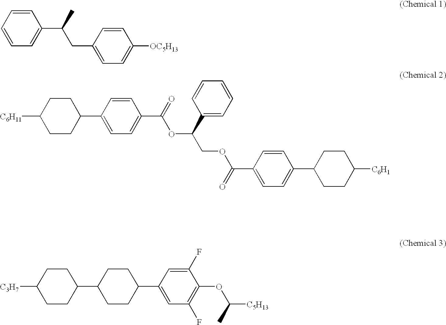
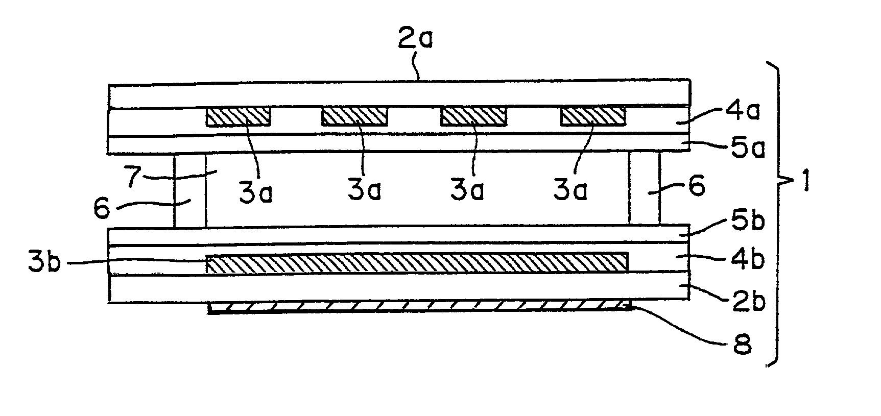
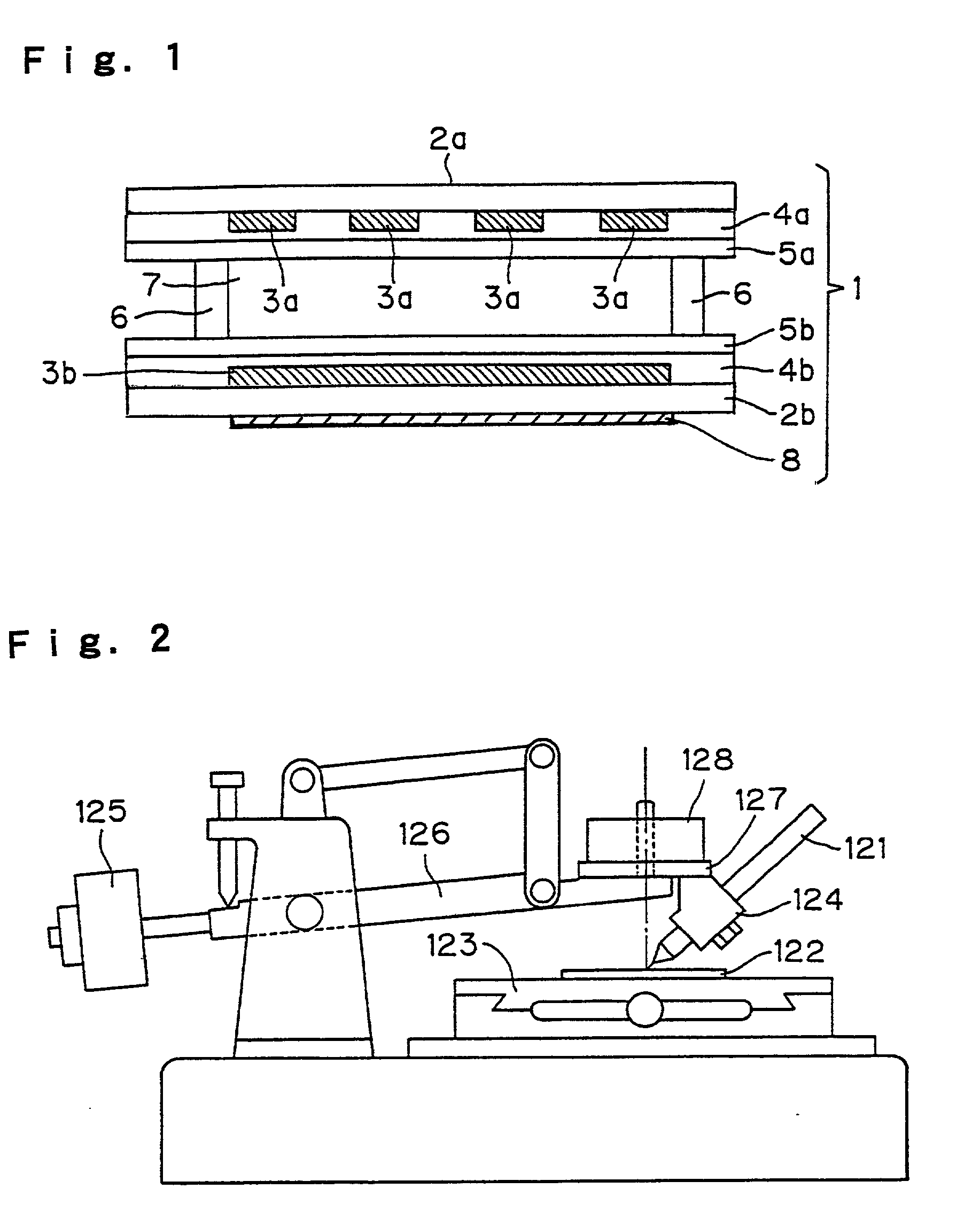
[0064] A liquid crystal optical element was prepared by the same method as in Example 1 except that a solution of polyimide resin RN-1286 manufactured by Nissan Chemical Industries, Ltd. was used. The line space was 10 .mu.m and the number of stripe electrodes was 160. The surface hardness of the resin layers was "3B".

[0065] First, initialization was performed by applying a relatively high voltage to liquid crystal corresponding to each pixel to render the liquid crystal to be HO; by eliminating the voltage in such state, and applying further a voltage which rendered the liquid crystal to be FC. After the initialization, a-line-at-a-time driving was performed in one round with 160 row electrodes and 160 column electrodes to display a character of "A", and then, the application of the voltage was stopped. As a result, a state that a character of "A" in a green color (PL) was displayed in a background of black color (FC), was provided. After the liquid crystal panel displaying a chara...


PUM

PropertyMeasurementUnit
temperatureaaaaaaaaaa
heat distortion temperatureaaaaaaaaaa
thicknessaaaaaaaaaa

Abstract

On substrates 2a, 2b of a chiral nematic liquid crystal optical element 1, transparent electrodes 3a, 3b and electrical insulation layers 4a, 4b are formed, and further, resin layers 5a, 5b having a pencil hardness of "B" or less are formed on the electrical insulation layers by a spin coating method so as to be in contact with a liquid crystal layer 7. When the surface hardness of the resin layers is to be measured, a glass substrate on which a resin layer is formed by screen-printing is prepared as a test piece, and the test piece is fitted to a pencil-scratching tester. The surface hardness is measured by scratching the test piece with two kinds of testing pencil selected from testing pencils having 17 grades of density.

Description

[0001] The entire disclosure of Japanese Patent Application No. 2000-402045 filed on Dec. 28, 2000, including specification, claims, drawings and summary are incorporated herein by reference in their entirely.[0002] 1. Field of the Invention[0003] The present invention relates to a liquid crystal optical element provided with liquid crystal which exhibits two or more optically stable states in a non-voltage-application time.[0004] 2. Description of the Background[0005] A chiral nematic liquid crystal optical element (hereinbelow, referred to as CL-LCD) has a phase-change type mode. It provides selective reflection in a planar state (hereinbelow, referred to as PL), and provides a scattering state in a focalconic state (hereinbelow, referred to as FC). By applying a predetermined voltage across the electrodes, the liquid crystal can be transformed into PL or FC. For example, when it is transformed from FC to PL, the liquid crystal is once rendered to be a homeotropic state (a state t...

Claims


Application Information

Patent Timeline
Patent Type & Authority Applications(United States)
IPC IPC(8): G02F1/1333G02F1/1337G02F1/137
CPCG02F1/133711G02F1/13718G02F1/1391G02F2001/133397G02F1/133397
Inventor NIIYAMA, SATOSHISUEHIRO, NORIKO
Owner ASAHI GLASS CO LTD
Why Eureka
Try Eureka