Method of depositing a copper seed layer which promotes improved feature surface coverage

a technology of feature surface coverage and copper seed layer, which is applied in the direction of vacuum evaporation coating, semiconductor/solid-state device details, coatings, etc., can solve the problems of cvd reactant deposition source contaminants, void spaces within the copper fill, and voids in the filled openings

Inactive Publication Date: 2002-06-06
APPLIED MATERIALS INC
View PDF0 Cites 5 Cited by
  • Summary
  • Abstract
  • Description
  • Claims
  • Application Information

AI Technical Summary

Problems solved by technology

A major problem encountered during the copper fill of a feature is the entrapment of void spaces within the copper fill.
For example, during copper fill of a feature such as a trench or via using chemical vapor deposition (CVD) there is a tendency to create voids within the filled opening; this is particularly true with regard to high aspect ratio features.
Other disadvantages of a CVD process are the contaminants from the CVD reactant deposition source which may be found in the deposited conductive material and the costs associated with use of this technology.
Filling of the copper feature with evaporated or sputtered copper is a cleaner process; however, the tendency to form voids still exists.
Further, evaporative deposition is a relatively slow process, decreasing production rates.
However, the reflow process is typically also a time consuming process.
However, such a reflow process presently is limited to aspect ratios of about 2:1 or less and typically requires more than a half hour of processing time.
However, if there are any discontinuities in the copper seed layer, voids are created within the copper fill where there are discontinuities in the seed layer.
Although it is possible to approach 100% of ionized species, typically the deposition rate decrease makes operation under the required conditions impractical.
We have discovered that when an inductively coupled plasma is used to increase ionization, an increase in RF power to the ionization source is not enough to obtain the desired percentage of ions in many cases.

Method used


Image

  • Method of depositing a copper seed layer which promotes improved feature surface coverage
  • Method of depositing a copper seed layer which promotes improved feature surface coverage
  • Method of depositing a copper seed layer which promotes improved feature surface coverage

Examples


example two

A Preferred Embodiment of the Present Invention

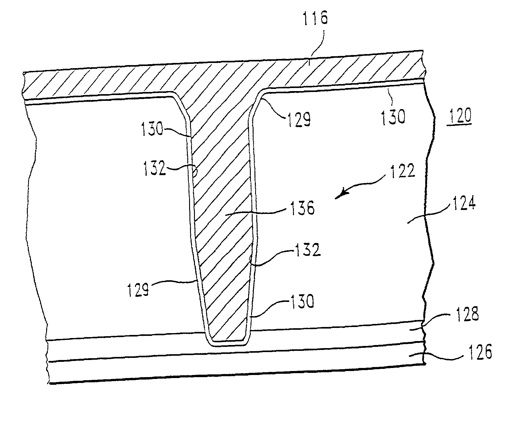
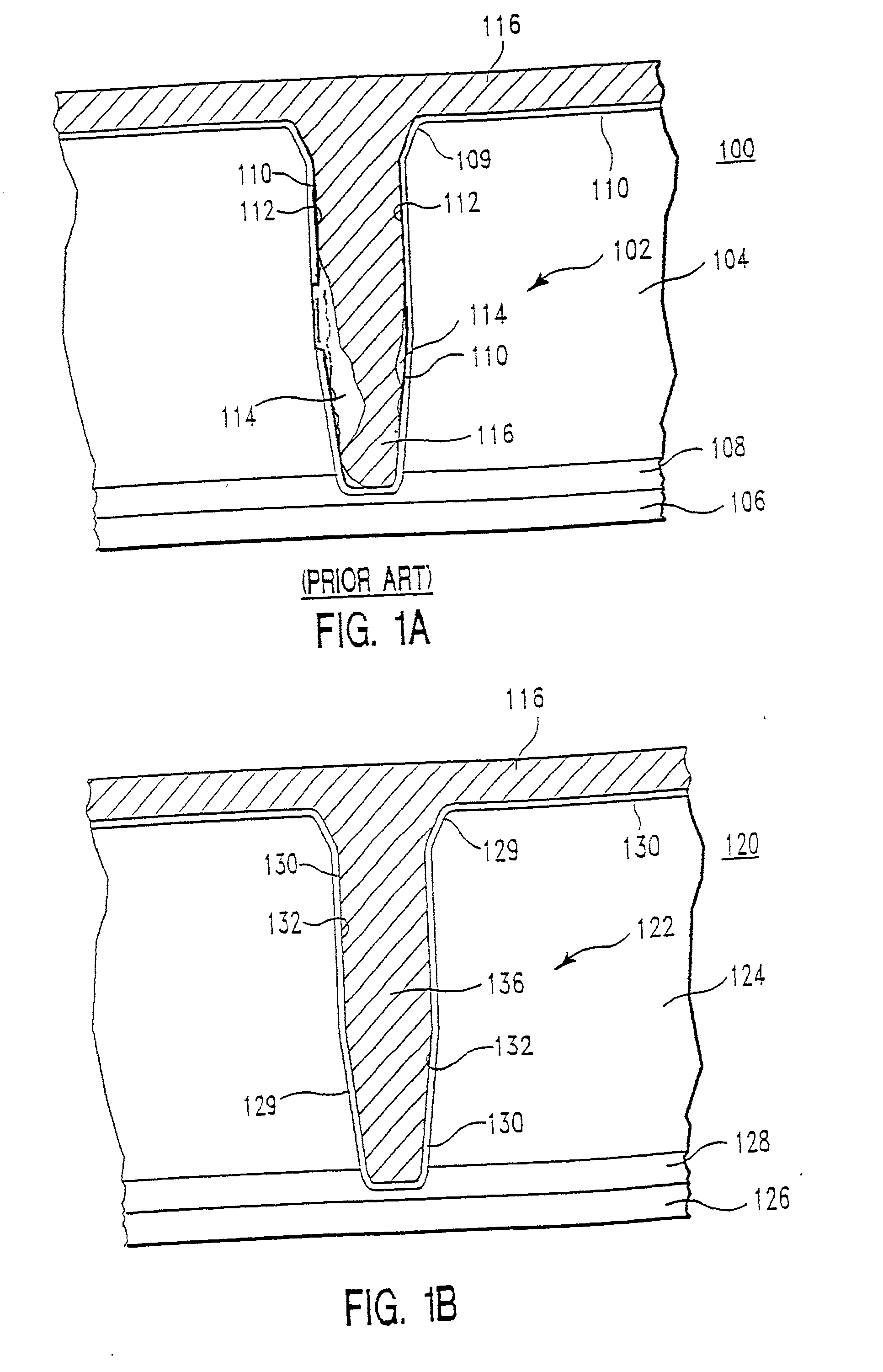
[0055] FIG. 1B illustrates a filled contact via prepared using the method of the present invention. FIG. 1B shows a schematic of a TEM cross-sectional view of a semiconductor structure 120 which includes a contact via 122 formed therein. The feature size of contact via 122 was 0.17 .mu.m, and the aspect ratio was about 7.

[0056] The preferred embodiments described herein were produced in a process chamber capable of processing a 200 mm diameter silicon wafer. The open surface 129 of contact via 122 was obtained by plasma etching of a layer of silicon oxide substrate 124 using techniques generally known in the art. A barrier layer 130 of tantalum nitride was applied using ion metal plasma-deposition sputtering conditions in the manner described with reference to FIG. 1A.

[0057] Subsequently, a copper seed layer 132 was applied using the following process conditions. The process chamber pressure was 60 mT; the plasma source power was 1 kW D...


PUM

PropertyMeasurementUnit
feature sizesaaaaaaaaaa
temperaturesaaaaaaaaaa
diameteraaaaaaaaaa

Abstract

We have discovered a method of improving step coverage of a copper seed layer deposited over a semiconductor feature surface which is particularly useful for small size features having a high aspect ratio. Using a contact via as an example of a high aspect ratio feature, we have demonstrated that despite previously-held views, it is possible to increase the copper seed layer coverage simultaneously at the bottom of the via and on the wall of the via by increasing the percentage of the depositing copper species which are ions. The percentage of species ionization which is necessary to obtain sufficient step coverage for the copper seed layer is a function of the aspect ratio of the feature. For features having a 0.25 mum or smaller feature size, an aspect ratio of about 3:1 requires that about 50% or more of the copper species be ions at the time of deposition on the substrate. As the aspect ratio increases to about 4:1, the percentage of species which are ions is preferably increased to between about 60% and 70%. When the aspect ratio is about 5:1 or greater, the percentage of species which are ions is preferably increased to greater than 80%. This increase in the percentage of copper species which are ionized can be achieved using techniques known in the art, such as, for example, laser ablation of the copper target, electron cyclotron resonance, hollow cathode, and applicants' preferred technique, an inductively coupled RF ion metal plasma. We have further discovered that when an inductively coupled plasma is used to increase ionization, an increase in power to the ionization source is not enough to obtain the desired percentage of ions in many cases. It is also necessary to increase the plasma gas pressure. Typically the plasma gas is argon, and the argon pressure in the copper seed layer deposition chamber is increased to fall within the range of about 20 to about 100 mT, preferably between about 30 mT and 70 mT.

Description

[0001] 1. Field of the Invention[0002] The present invention pertains to a method for depositing a copper seed layer having improved step coverage over a feature surface, and to the improved feature structure which is obtained using the method.[0003] 2. Brief Description of the Background Art[0004] Due to the difficulty in etching a copper film to provide a desired semiconductor interconnect pattern, one of the preferred methods of providing copper interconnects is the damascene process, which requires the filling of embedded trenches and / or vias.[0005] A typical damascene process for producing a multilevel structure having feature sizes in the range of 0.5 micron (.mu.) or less would include: blanket deposition of a dielectric material over a semiconductor surface; patterning of the dielectric material to form openings; deposition of a conductive material over the surface of the dielectric material in sufficient amount to fill the openings; and removal of excessive conductive mater...

Claims


Application Information

Patent Timeline
Patent Type & Authority Applications(United States)
IPC IPC(8): C23C14/14C23C14/40H01L21/28H01L21/285H01L21/768H01L23/532
CPCH01L21/2855H01L21/76877H01L23/53233H01L23/53238H01L2924/0002H01L2924/00H01L21/28
Inventor HASHIM, IMRANZHANG, HONG-MEIFORSTER, JOHN C.
Owner APPLIED MATERIALS INC
Why Eureka
Try Eureka