Method of forming a metal wiring in a semiconductor device

a metal wiring and semiconductor technology, applied in the direction of semiconductor/solid-state device details, chemical vapor deposition coating, coating, etc., can solve the problems of low efficiency of cvd method, low deposition speed and cost, and shorten the lifetime of metal wiring, so as to achieve the effect of easy forming a copper wir

Inactive Publication Date: 2002-04-25
SK HYNIX INC
View PDF0 Cites 5 Cited by
  • Summary
  • Abstract
  • Description
  • Claims
  • Application Information

AI Technical Summary

Benefits of technology

0006] A method of forming a metal wiring in a semiconductor device is disclosed that is capable of performing a selective deposition process of copper using a copper precursor and thus easily forming a copper wiring in an ult...

Problems solved by technology

As the size of a contact is reduced and the aspect ratio is increased for rapid high performance of next-generation semiconductor devices, a metal wiring using aluminum has a problem in that the EM characteristic in which the lifetime of the metal wiring is shortened due to high current density.
As the electroplating method, however, has a limitation in filling in case of ultra-fine structure, interest in a copper wiring filling using a CVD method h...

Method used


Image

  • Method of forming a metal wiring in a semiconductor device
  • Method of forming a metal wiring in a semiconductor device
  • Method of forming a metal wiring in a semiconductor device

Examples


Embodiment Construction

[0010] The disclosed method will be described in detail by way of a preferred embodiment with reference to accompanying drawings.

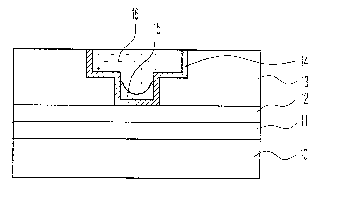
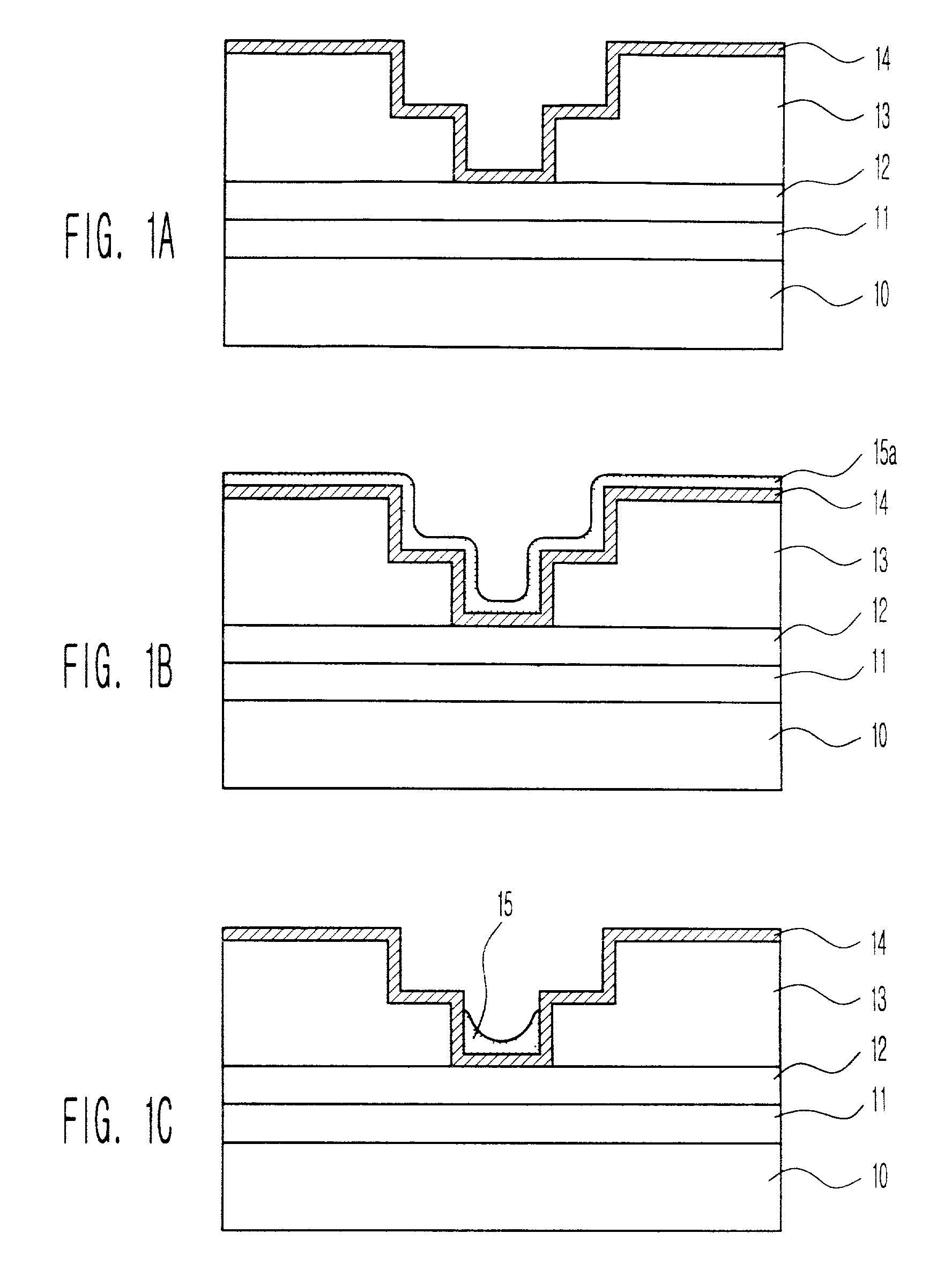
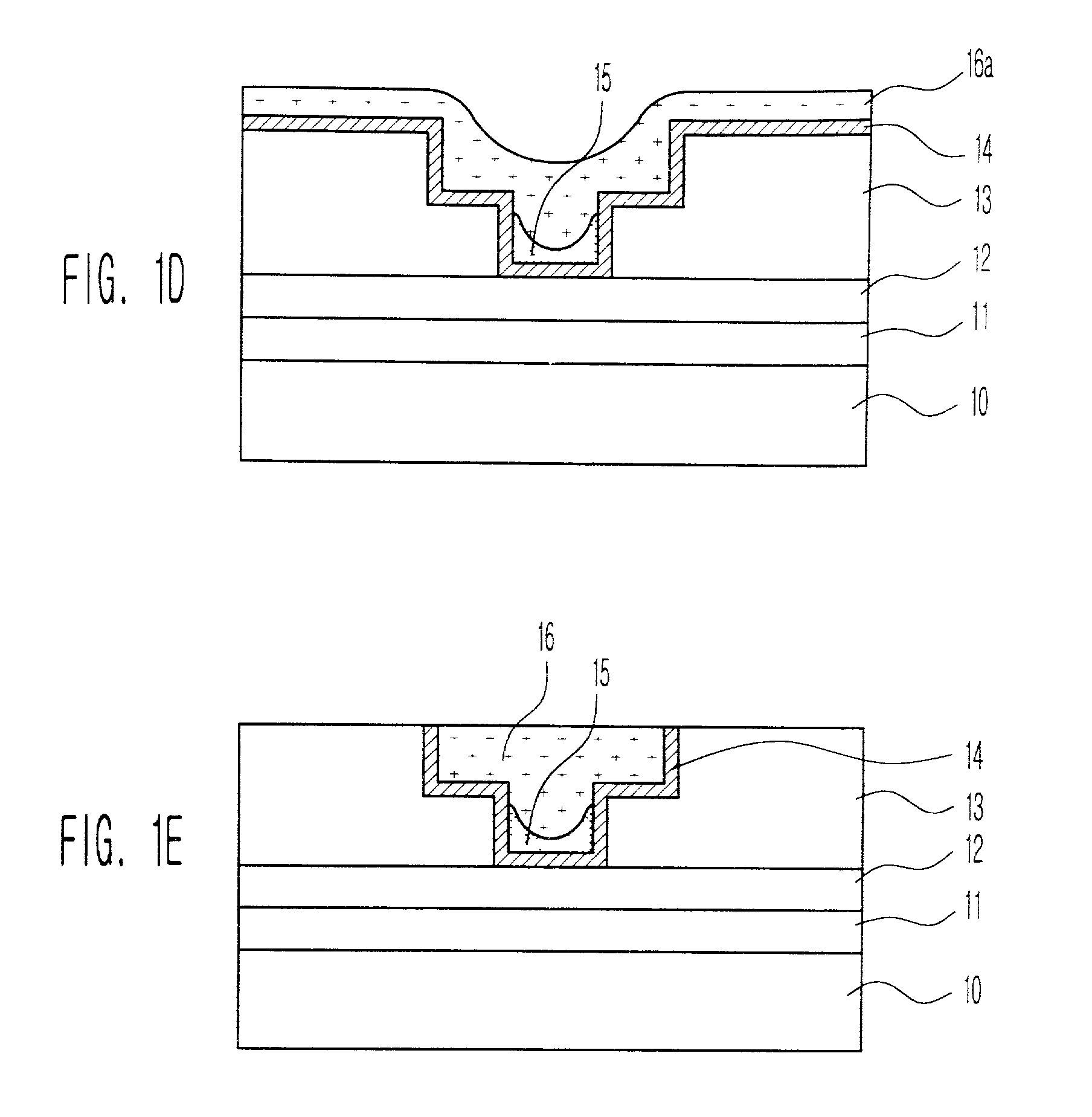
[0011] Referring now to FIG. 1A, an insulating film 1, a lower metal layer 12 and a second insulating film 13 are sequentially formed on a semiconductor substrate 10 in which various components for forming a semiconductor device is formed. A damascene pattern consisting of a trench and / or via is then formed in the second insulating film. Next, a cleaning is performed to remove an oxide layer remaining on the surface of the lower metal layer 12 exposed by the damascene pattern. Thereafter, a diffusion prevention film 14 is formed on the second insulating film 13 including the damascene pattern. The surface of the diffusion prevention film 14 is exposed to a plasma process in order to facilitate formation of a subsequent chemical enhancer layer 15a or a seed layer 15a which is formed in thickness ranging from about 50 to about 500 .ANG. using copper (Cu) on ...


PUM

PropertyMeasurementUnit
Timeaaaaaaaaaa
Timeaaaaaaaaaa
Pressureaaaaaaaaaa

Abstract

A method of forming a metal wiring in a semiconductor device. In order to overcome the limitation of copper filling into the damascene pattern formed on an insulating film using copper as a metal wiring, a chemical enhancer layer is formed on the damascene pattern which is then filled with copper by depositing copper by means of MOCVD method using a copper precursor. The chemical enhancer is exposed to a plasma process or radical plasma process so that it remains only within a bottom portion of the damascene pattern. Therefore, a selective copper deposition within the damascene pattern is provided to accelerate the deposition speed of copper by CECVD method, thus overcoming the limitation of slow and incomplete copper filling for ultra-fine structures.

Description

[0001] 1. Technical Field[0002] A method of forming a metal wiring in a semiconductor device is disclosed. More particularly, the present invention relates to a method of forming a metal wiring in a semiconductor device by which a chemical enhancer layer is formed and copper filled in the damascene pattern by means of selective deposition method using a copper precursor to form a copper wiring.[0003] 2. Description of the Prior Art[0004] As the size of a contact is reduced and the aspect ratio is increased for rapid high performance of next-generation semiconductor devices, a metal wiring using aluminum has a problem in that the EM characteristic in which the lifetime of the metal wiring is shortened due to high current density. In order to overcome this problem, a study has been made on a wiring material having low resistance. Recently, wiring material using copper (Cu) has been studied. Also, the commercialization of electroplating method considering cost and deposition speed has ...

Claims


Application Information

Patent Timeline
IPC IPC(8): C23C16/04C23C16/18H01L21/285H01L21/3205H01L21/768H01L23/52
CPCC23C16/04H01L21/76879H01L21/76838C23C16/18H01L21/28
Inventor PYO, SUNG GYU
Owner SK HYNIX INC
Why Eureka
Try Eureka