
Parallel opto-electric structure for high sensitivity and wide bandwidth optical transceiver

a transceiver and optical transceiver technology, applied in electromagnetic receivers, electromagnetic transmission, transmission, etc., can solve the problems of parasitic capacitance of pin diodes, difficult to achieve high sensitivity and wide bandwidth in a single large area pin diodes, and suffer from conventional ir receivers

Inactive Publication Date: 2002-01-10
IBM CORP
View PDF0 Cites 12 Cited by
  • Summary
  • Abstract
  • Description
  • Claims
  • Application Information

AI Technical Summary

Problems solved by technology

The design of any conventional IR receiver suffers from PIN diode parasitic capacitance when both high sensitivity and wide bandwidth are required.
It can be seen from equations (3) and (9) that it is very difficult to achieve both high sensitivity and a wide bandwidth in a single large area PIN diode.

Method used


Image

  • Parallel opto-electric structure for high sensitivity and wide bandwidth optical transceiver
  • Parallel opto-electric structure for high sensitivity and wide bandwidth optical transceiver
  • Parallel opto-electric structure for high sensitivity and wide bandwidth optical transceiver

Examples


Embodiment Construction

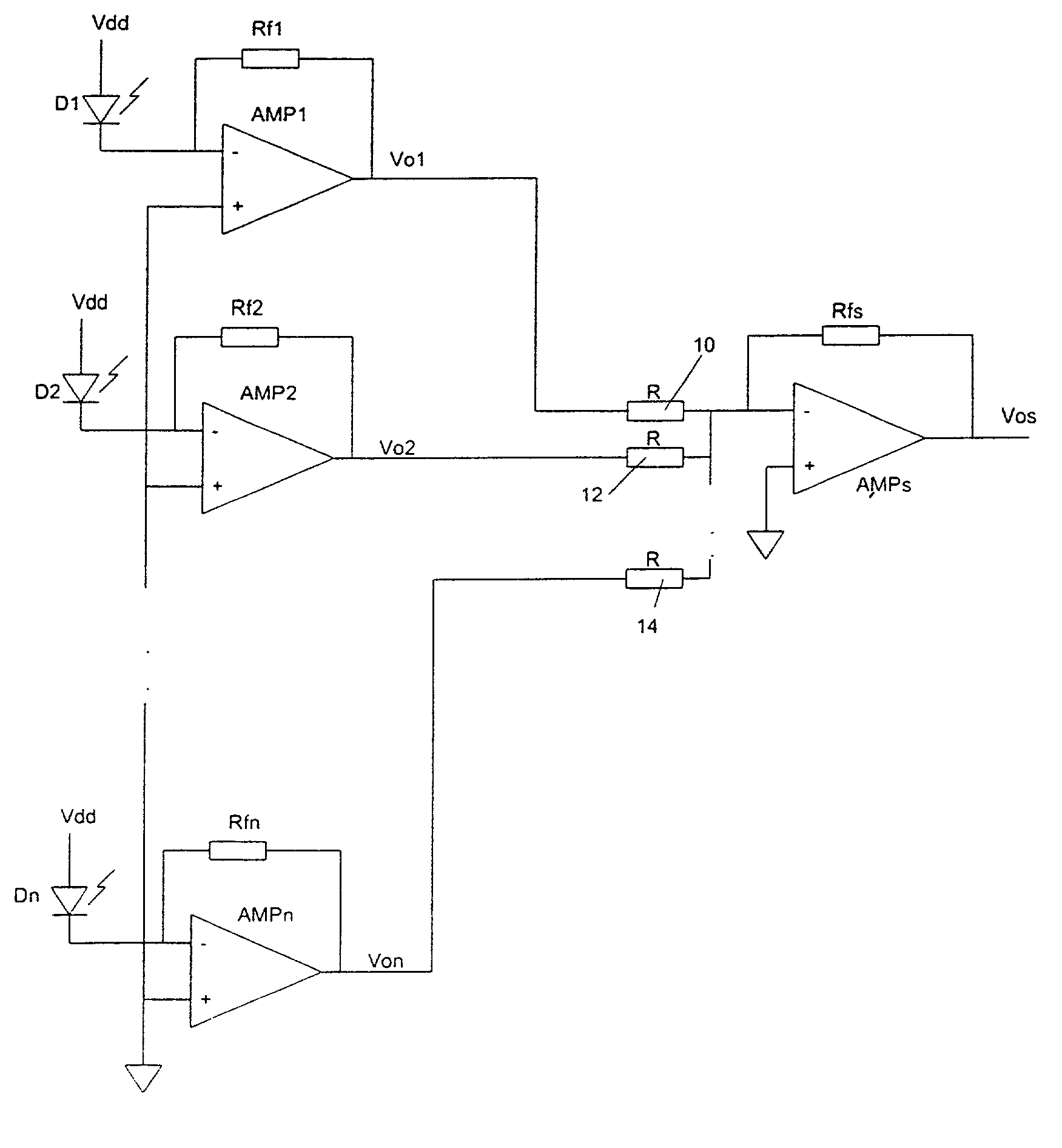
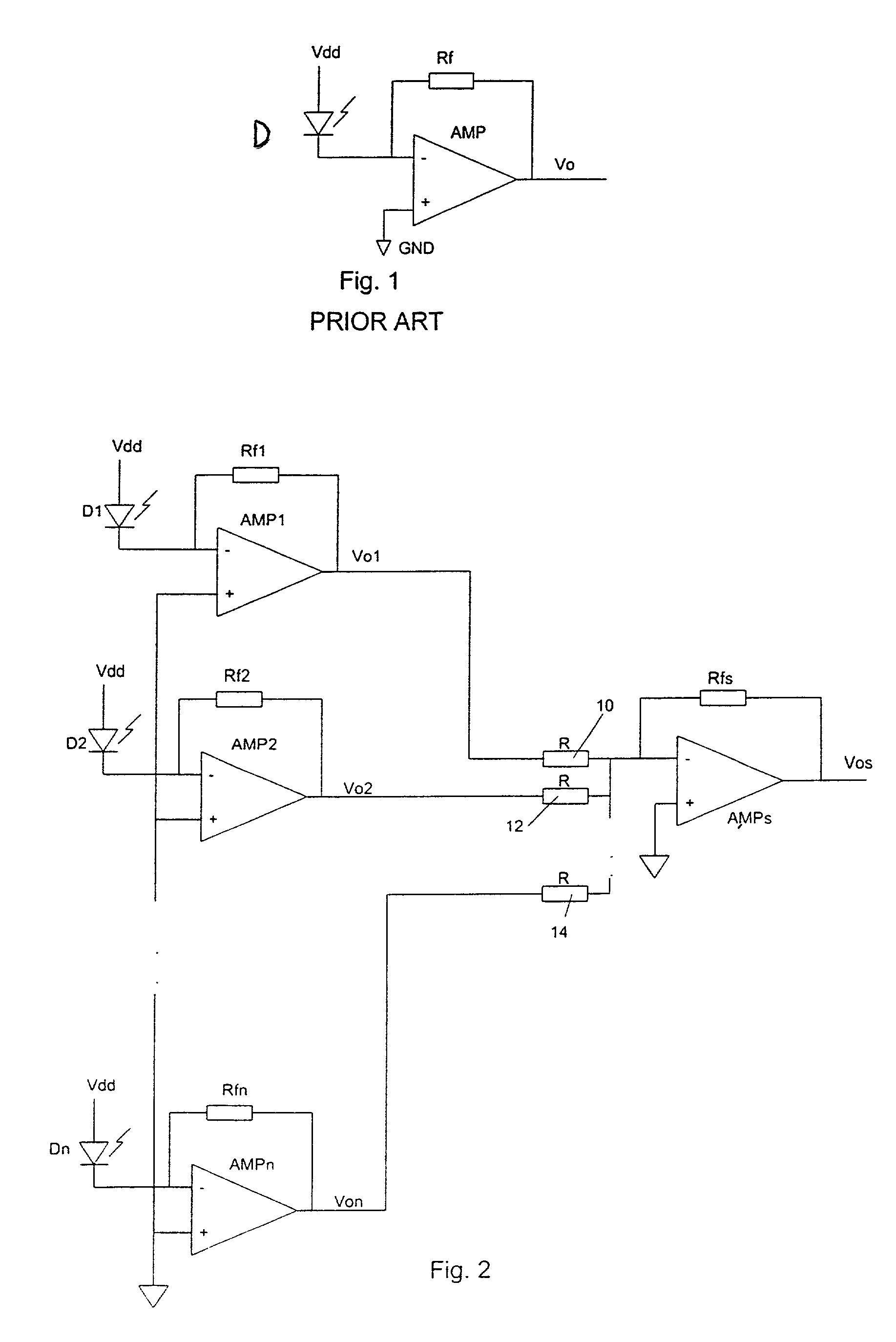
[0029] FIG. 2 illustrates a preferred embodiment of an optical receiver circuit according to the invention.

[0030] In FIG. 2, a plurality of photodiodes (e.g., in the preferred embodiment PIN diodes P.sub.1, P.sub.2 . . . P.sub.N) have their anodes connected to a voltage supply V.sub.dd to supply a bias voltage across the diodes P.sub.1, P.sub.2 . . . P.sub.N. The cathode of a first PIN diode P.sub.1 is connected to the inverting input of a first element transimpedance amplifier (unreferenced), including an operational amplifier AMP.sub.1 having a resistance element such as feedback resistor R.sub.1 with a resistance R.sub.f1 connecting the output of the operational amplifier AMP.sub.1 to the inverting input of the operational amplifier AMP.sub.1.

[0031] Similarly, the cathode of a second PIN diode P.sub.2 is connected to the inverting input of a second element transimpedance amplifier (unreferenced) including an operational amplifier AMP.sub.2 having a feedback resistor R.sub.2 with ...


PUM


Abstract

An optical receiver circuit including a plurality of PIN diodes, each associated with a dedicated element transimpedance amplifier, the outputs of the element transimpedance amplifiers being connected to a summing amplifier which sums the voltages output from the element transimpedance amplifiers. The optical receiver circuit provides the same output voltage value as a single large PIN diode having an active area comparable to the sum of the active areas of the smaller PIN diodes, and thus has the same high sensitivity as the single large PIN diode but a much wider bandwidth.

Description

[0001] 1. Field of the Invention[0002] The present invention relates to an optical transceiver, and more particularly to a receiver circuit for an optical transceiver having a plurality of photodiodes.[0003] 2. Description of the Related Art[0004] An optical receiver converts optical pulses to corresponding electrical signals. The optical receiver in an infrared (IR) optical transceiver typically utilizes an IR-sensitive PIN diode, which emits an electric current in proportion to the intensity of infrared light striking the active area of the diode.[0005] For example, FIG. 1 illustrates the general structure of a conventional optical receiver circuit for an IR transceiver. A PIN diode D has its anode connected to the power Supply V.sub.dd to create a bias voltage across the PIN diode D, and its cathode connected to the inverting input of an operational amplifier AMP. A feedback resistor R.sub.f is connected between the output and the inverting input, so that the operational amplifie...

Claims


Application Information

Patent Timeline
IPC IPC(8): H04B10/69
CPCH04B10/69H04B10/6932
Inventor FENG, KAI D.
Owner IBM CORP
Learn More