Nanostructure based display devices

a display device and nanostructure technology, applied in the field of nanostructure based display devices, can solve the problems of 10 micron) layer and minimal net benefit in color gamut coverag

Active Publication Date: 2022-11-22
SHOEI CHEM IND CO LTD
View PDF4 Cites 0 Cited by
  • Summary
  • Abstract
  • Description
  • Claims
  • Application Information

AI Technical Summary

Benefits of technology

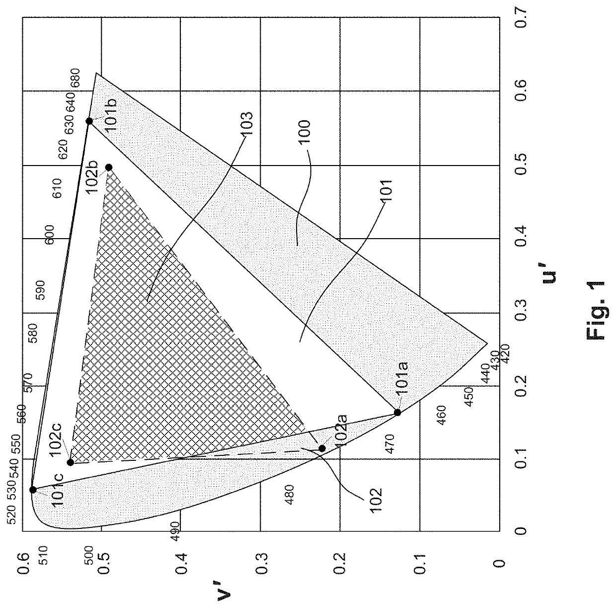
[0007]Accordingly, there is need for display devices with improved color gamut coverage through both higher absorption in the color conversion layers and a longer wavelength source light.

Problems solved by technology

This can be difficult in a thin (about 3-10 micron) layer using a NS film due to its limited optical density in such a layer.
Thus, there is minimal net benefit in color gamut coverage by simply shifting the wavelength of the source light.

Method used


Image

  • Nanostructure based display devices
  • Nanostructure based display devices
  • Nanostructure based display devices

Examples


Embodiment Construction

[0080]Although specific configurations and arrangements may be discussed, it should be understood that this is done for illustrative purposes only. A person skilled in the pertinent art will recognize that other configurations and arrangements can be used without departing from the spirit and scope of the present invention. It will be apparent to a person skilled in the pertinent art that this invention can also be employed in a variety of other applications beyond those specifically mentioned herein. It should be appreciated that the particular implementations shown and described herein are examples and are not intended to otherwise limit the scope of the application in any way.

[0081]It is noted that references in the specification to “one embodiment,”“an embodiment,”“an example embodiment,” etc., indicate that the embodiment described may include a particular feature, structure, or characteristic, but every embodiment may not necessarily include the particular feature, structure, ...


PUM

PropertyMeasurementUnit
peak wavelengthaaaaaaaaaa

Abstract

Embodiments of a display device are described. A display device includes a backlight unit having a light source and a liquid crystal display (LCD) module. The light source is configured to emit a primary light having a first peak wavelength. The LCD module includes a first sub-pixel having a phosphor film and a second sub-pixel having a non-phosphor film. The phosphor film is configured to receive a first portion of the primary light and to convert the first portion of the primary light to emit a secondary light having a second peak wavelength that is different from the first peak wavelength. The non-phosphor film is configured to receive a second portion of the primary light and to optically modify the second portion of the primary light to emit an optically modified primary light having a third peak wavelength that is different from the first and second peak wavelengths.

Description

CROSS REFERENCE TO RELATED APPLICATIONS[0001]This application incorporates by reference in their entirety U.S. Provisional Appl. No. 62 / 764,773, filed Aug. 16, 2018.BACKGROUND OF THE INVENTIONField[0002]The present invention relates to display devices including phosphor films having luminescent nanostructures such as quantum dots (QDs).Background[0003]Luminescent nanostructures (NSs) such as quantum dots (QDs) represent a class of phosphors that have the ability to emit light at a single spectral peak with narrow line width, creating highly saturated colors. It is possible to tune the emission wavelength based on the size of the NSs. The NSs are used to produce a NS film that may be used as a color down conversion layer in display devices (e.g., liquid crystal display (LCD) device, organic light emitting diode (OLED) display device, micro-LED display device, or quantum dot LED display device). The use of a color down conversion layer in emissive displays can improve the system effic...

Claims


Application Information

Patent Timeline
Patent Type & Authority Patents(United States)
IPC IPC(8): G02F1/13357G02F1/1335
CPCG02F1/133603G02F1/133504G02F1/133509G02F1/133528G02F2202/36G02F1/133602G02F1/133615G09F9/35G02F1/133614G02F1/133617
Inventor LEE, ERNEST CHUNG-WEIHOTZ, CHARLES
Owner SHOEI CHEM IND CO LTD
Why Eureka
Try Eureka