
Array substrate having film layer disconnected at corresponding groove and OLED display panel having the same, and mask

a technology of oled display panel and substrate, applied in vacuum evaporation coating, coating, chemical vapor deposition coating, etc., can solve the problems of shadow effect, unavoidable use of mask, and pose certain risks for subsequent device cutting and reliability verification

Active Publication Date: 2022-10-11
WUHAN CHINA STAR OPTOELECTRONICS SEMICON DISPLAY TECH CO LTD
View PDF5 Cites 0 Cited by
  • Summary
  • Abstract
  • Description
  • Claims
  • Application Information

AI Technical Summary

Benefits of technology

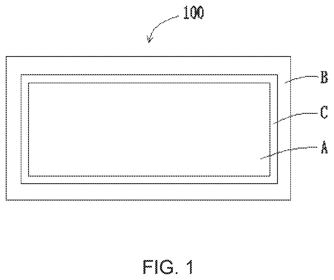
[0006]The present invention provides an array substrate, an OLED display panel, and a mask, which can solve adverse effects caused by film layers disposed in shadow regions on film layers of a predetermined film-forming region, and resolve shadow effects generated in CVD processes.
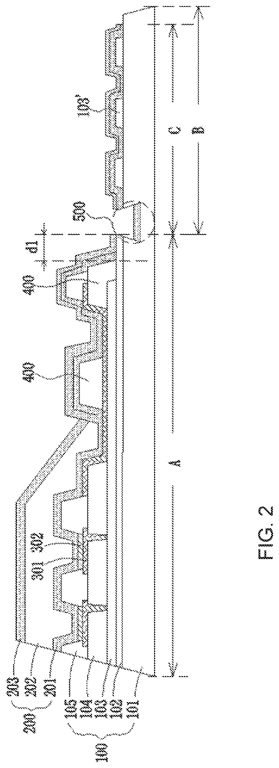
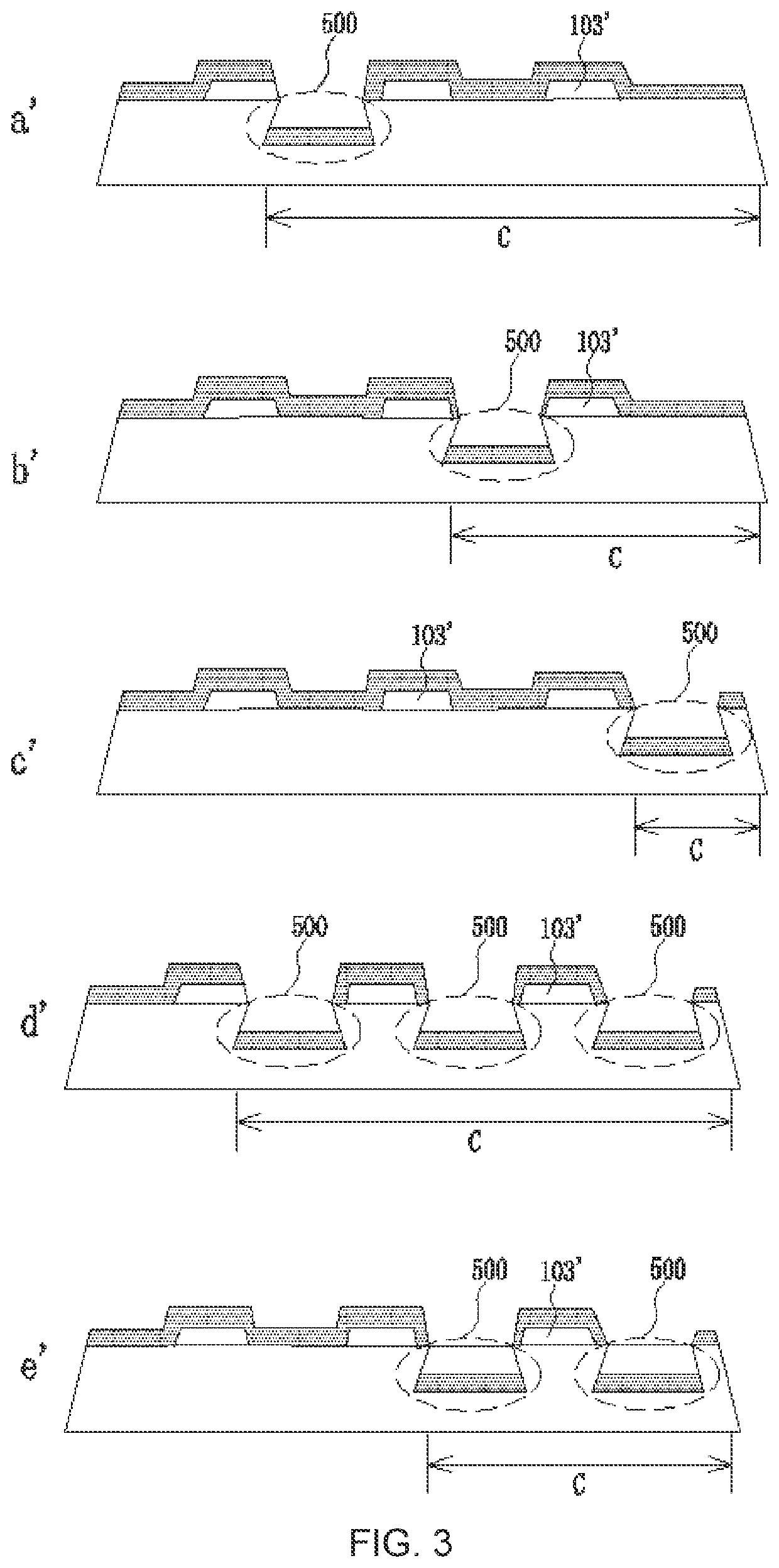
[0027]The beneficial effect of the present invention is: compared with current display panels, an array substrate, an OLED display panel, and a mask provided in the present invention are formed by providing grooves or protrusions in corresponding shadow regions of the array substrate. A film layer on the substrate is disconnected at corresponding grooves or protrusions to form a discontinuous film, thereby preventing the film layer disposed in the shadow regions from causing adverse effect on the film layer of a predetermined film-forming region. In addition, the present invention further processes an edge of openings of the mask to achieve a purpose of reducing areas of the shadow regions, thereby facilitating a design of narrow borders of display panels and reducing effect of shadow effect.

Problems solved by technology

However, there is an unavoidable problem with use of a mask, which is called shadow effect.
It poses certain risks for subsequent device cutting and reliability verification.
However, the shadow effect in CVD film formation process is unavoidable in the current industry.
Therefore, current technologies have defects and urgently need improvement.

Method used


Image

  • Array substrate having film layer disconnected at corresponding groove and OLED display panel having the same, and mask
  • Array substrate having film layer disconnected at corresponding groove and OLED display panel having the same, and mask
  • Array substrate having film layer disconnected at corresponding groove and OLED display panel having the same, and mask

Examples


Embodiment Construction

[0034]The following description of the various embodiments is provided with reference to the accompanying drawings. Directional terms, such as upper, lower, front, back, left, right, inner, outer, and lateral side, mentioned in the present invention are only for reference. Therefore, the directional terms are used for describing and understanding rather than limiting the present invention. In the figures, units having similar structures are used for the same reference numbers.

[0035]The present invention is directed to a current display panel. Current films formed by chemical vapor deposition (CVD) methods must be assisted by masks to pattern film layers. However, there is an unavoidable problem with the use of a mask, which is called shadow effect. The so-called shadow is due to existence of a certain gap between the mask and a substrate during film formations, and plasma will enter a non-open region at an edge of the mask to form a film. The thin film in the region is thinner than ...


PUM

PropertyMeasurementUnit
depthaaaaaaaaaa
distanceaaaaaaaaaa
widthaaaaaaaaaa

Abstract

The present invention provides an array substrate, an OLED display panel, and a mask. The array substrate includes a predetermined film-forming region and a non-film forming region. The non-film forming region is provided with a shadow region close to the predetermined film-forming region. An actual film forming region of a film layer to be formed on the array substrate includes the predetermined film-forming region and the shadow region. The array substrate is provided with a groove or a protrusion in the corresponding shadow region, so that the film layer is disconnected at the corresponding groove or the protrusion to form a discontinuous film.

Description

RELATED APPLICATIONS[0001]This application is a National Phase of PCT Patent Application No. PCT / CN2020 / 074855 having International filing date of Feb. 12, 2020, which claims the benefit of priority of Chinese Patent Application No. 201910934726.5 filed on Sep. 29, 2019. The contents of the above applications are all incorporated by reference as if fully set forth herein in their entirety.FIELD AND BACKGROUND OF THE INVENTION[0002]The present application relates to the field of display technologies, and in particular, to an array substrate, an OLED display panel, and a mask.[0003]Compared with traditional liquid crystal displays, AMOLEDs have advantages of high contrast, wide viewing angles, wide color gamut, and high resolution. With expansion of OLED application fields, new application fields will have increasingly higher requirements for OLED devices, especially requirements for encapsulated inorganic films.[0004]Current encapsulated inorganic films formed by chemical vapor depos...

Claims


Application Information

Patent Timeline
Patent Type & Authority Patents(United States)
IPC IPC(8): H01L51/52H01L27/32H01L51/56C23C16/04
CPCH01L51/5253H01L27/3244H01L51/56C23C16/042H10K59/00H10K59/88H10K59/12C23C14/042H10K50/80H10K50/844H10K71/00
Inventor ZHANG, XINGYONG
Owner WUHAN CHINA STAR OPTOELECTRONICS SEMICON DISPLAY TECH CO LTD
Learn More