Phononic devices and methods of manufacturing thereof

a phononic device and phononic technology, applied in the field of phononic devices with a plurality of functions, can solve the problem of high scalable kinetic inductance detectors (kids)

Active Publication Date: 2022-08-23
NASA
View PDF2 Cites 0 Cited by
  • Summary
  • Abstract
  • Description
  • Claims
  • Application Information

AI Technical Summary

Benefits of technology

The present invention is about a method of manufacturing phononic devices that can be used in highly sensitive cryogenic detectors. These devices use phononic crystals to reduce the loss of athermal phonons, which results in lower noise and higher sensitivity detectors. The fabrication process also increases the lifetime of the detectors, reducing the noise equivalent power without sacrificing scalability. The invention can be used to manufacture various phononic devices, such as kinetic inductance detectors and TES detectors. By using phononic crystals, the invention achieves better thermal isolation and reduces the NEP, making it suitable for imaging and spectroscopic studies.

Problems solved by technology

Kinetic inductance detectors (KIDs) are highly scalable to large format arrays but are not as sensitive as transition edge sensor (TES) bolometers, and have not demonstrated noise equivalent power (NEP) less than 10−19 W / rt-Hz, and are limited by the generation recombination rate of quasi-particles (qp) in the superconducting film.

Method used


Image

  • Phononic devices and methods of manufacturing thereof
  • Phononic devices and methods of manufacturing thereof
  • Phononic devices and methods of manufacturing thereof

Examples


Embodiment Construction

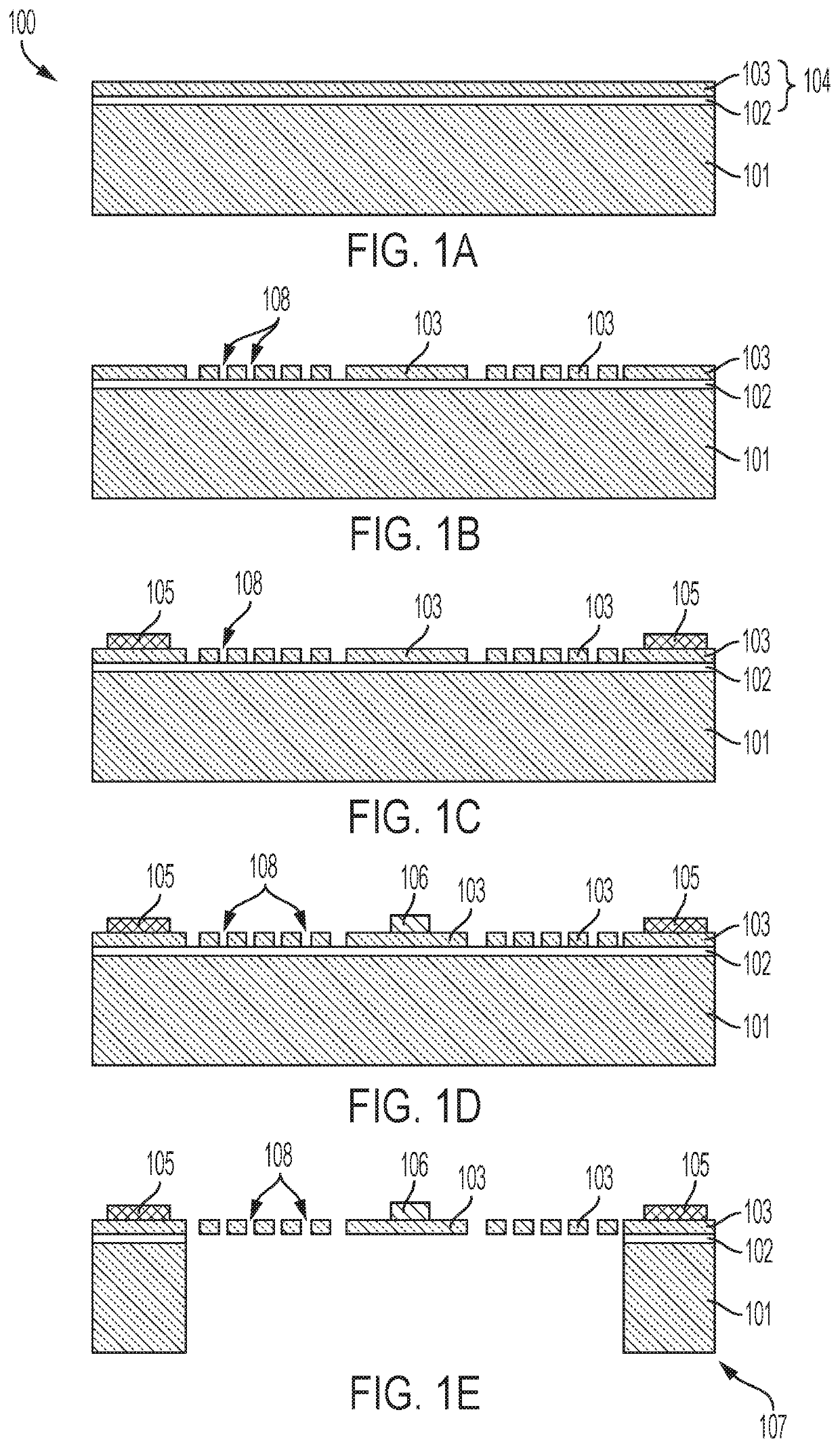
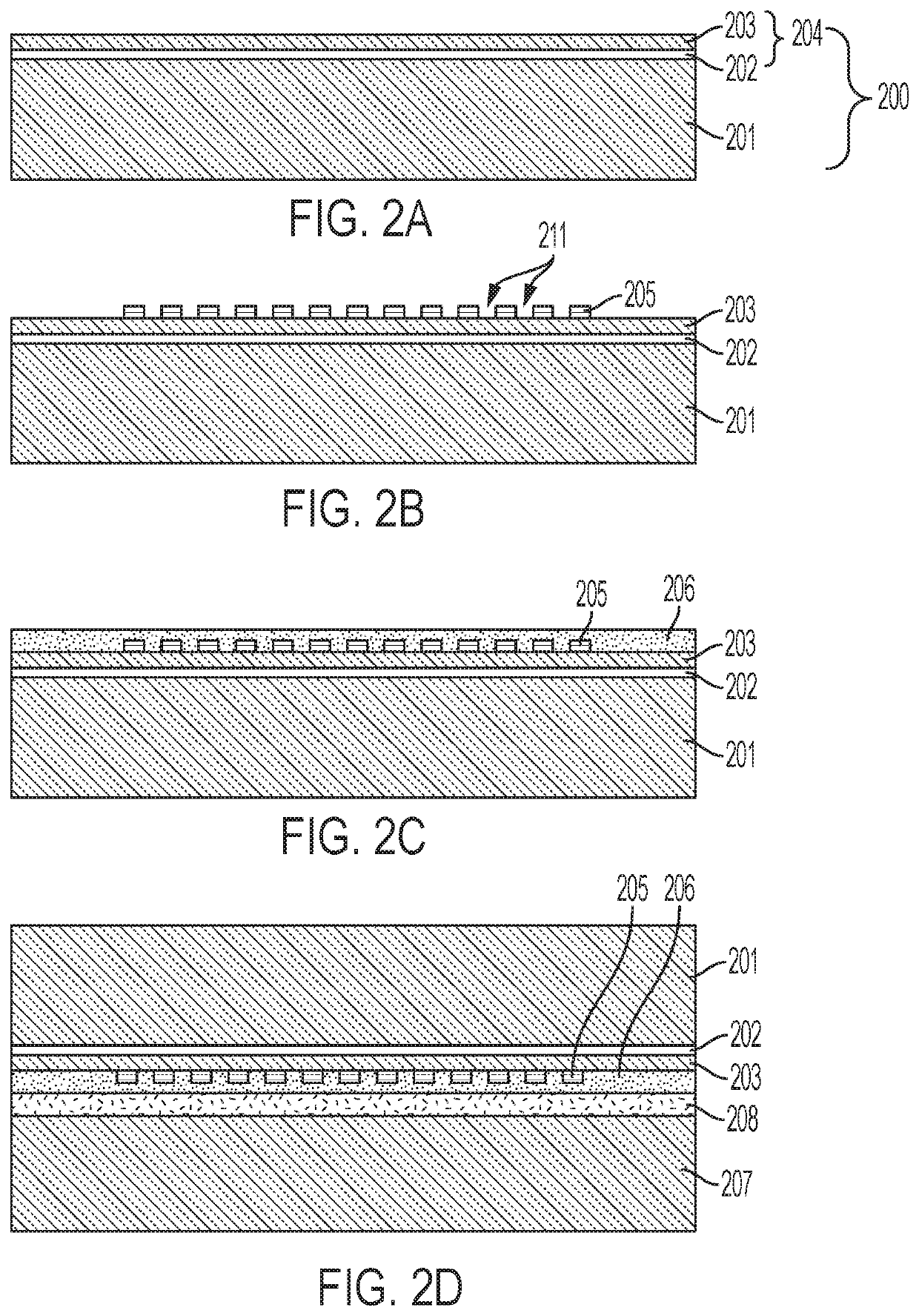
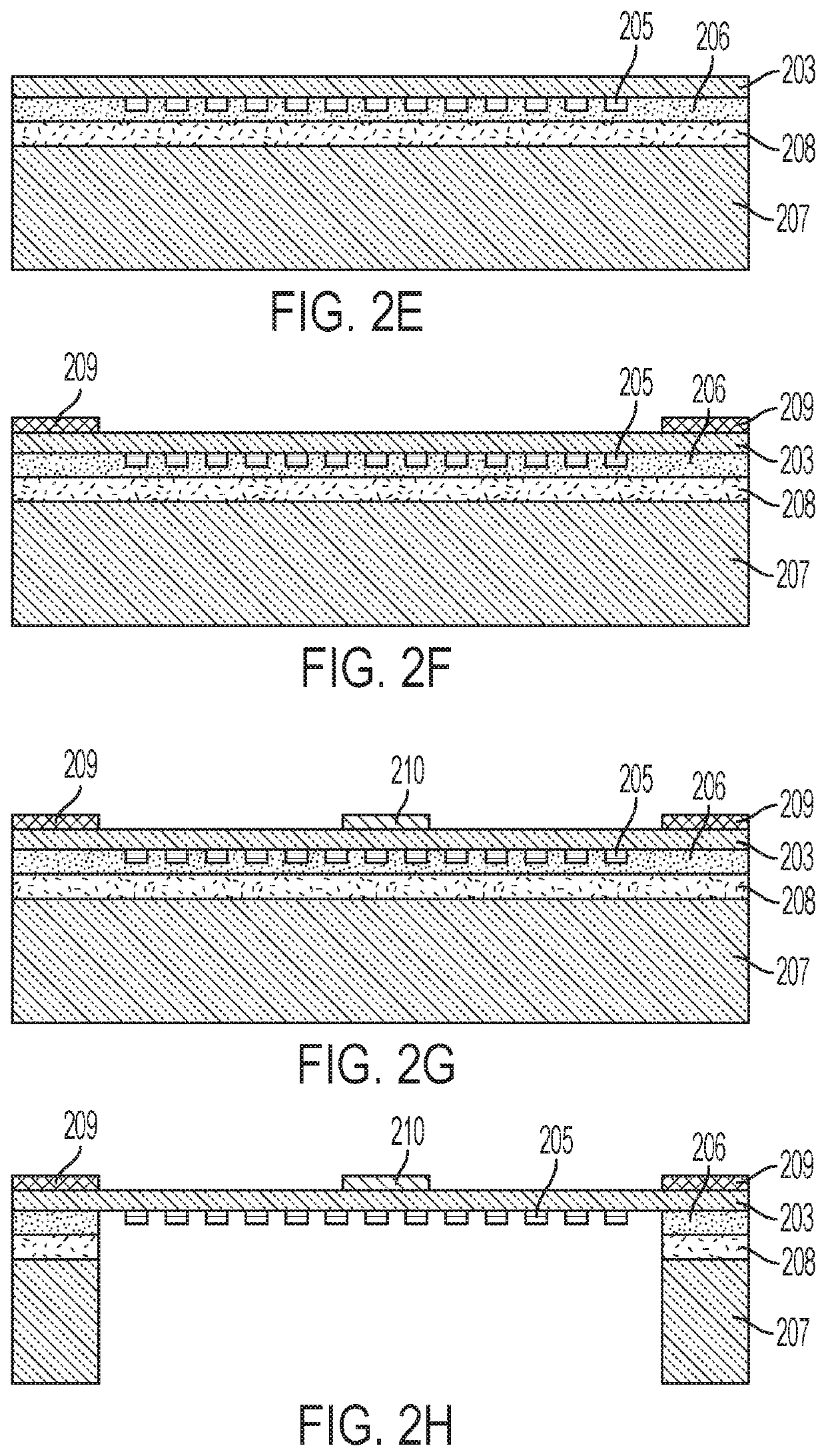
[0069]The present invention relates to a plurality of phononic devices and a method of manufacturing thereof. In one embodiment, highly sensitive superconducting cryogenic detectors integrate phononic crystals into their architecture. The phononic structures are designed to reduce the loss of athermal phonons from the superconductor, resulting in lower noise and higher sensitivity detectors. This fabrication process increases the qp generation recombination lifetime, thus, reducing the noise equivalent power (NEP) without sacrificing the scalability. A plurality of phononic devices, such as a kinetic inductance detector (KID) or transition edge sensor (TES) can be manufactured according to the methods of the present invention. Additionally, a method for incorporating a resonant backshort is disclosed in the present invention.

[0070]It is anticipated that a photon noise limited sub-mm / far-IR cold telescope in space will require detectors with noise equivalent power (NEP) less than 1×1...


PUM

PropertyMeasurementUnit
impedanceaaaaaaaaaa
pressureaaaaaaaaaa
Inductanceaaaaaaaaaa

Abstract

The present invention relates to a plurality of phononic devices and a method of manufacturing thereof. In one embodiment, highly sensitive superconducting cryogenic detectors integrate phononic crystals into their architecture. The phononic structures are designed to reduce the loss of athermal phonons, resulting in lower noise and higher sensitivity detectors. This fabrication process increases the qp generation recombination rate, thus, reducing the noise equivalent power (NEP) without sacrificing the scalability. A plurality of phononic devices, such as a kinetic inductance detector (KID), a transition edge sensor (TES) bolometer, and quarterwave backshort, can be manufactured according to the methods of the present invention.

Description

CROSS-REFERENCE TO RELATED APPLICATIONS[0001]The present application claims priority from U.S. Provisional Patent Application No. 62 / 834,572, filed Apr. 16, 2019, the contents of which are herein incorporated by reference in their entirety. The present invention is related to co-pending U.S. Patent Application entitled “Phononic-Isolated Kinetic Inductance Detector and Fabrication Method Thereof”, filed Sep / 27, 2019, U.S. patent application Ser. No. 16 / 585,559, and co-pending U.S. Patent Application entitled “Cryogenic Detector with Integrated Backshort and Method of Manufacturing Thereof”, filed Sep. 27, 2019, U.S. patent application Ser. No. 16 / 585,509, the contents of which are herein incorporated by reference in their entirety.ORIGIN OF THE INVENTION[0002]The invention described herein was at least in-part made by an employee of the United States Government and may be manufactured or used by or for the Government of the United States of America for governmental purposes without...

Claims


Application Information

Patent Timeline
Patent Type & Authority Patents(United States)
IPC IPC(8): H01L39/00H01L39/24H03H9/02H01L39/22H01L39/08
CPCH01L39/2406H01L39/08H01L39/22H03H9/02102G01J5/20G01J2005/208G01J5/34G01J5/0853G01J5/22H10N60/10H10N60/20H10N60/83H10N60/85H10N60/0156H10N60/0884
Inventor DENIS, KEVINROSTEM, KARWANWOLLACK, EDWARDWILLIAMS, ELISSA
Owner NASA
Why Eureka
Try Eureka