Electromagnetic interference (EMI) shielding member and electronic device including the same

a shielding member and electromagnetic interference technology, applied in the direction of shielding materials, printed circuit non-printed electric components association, electrical apparatus contruction details, etc., can solve the problems of high contact resistance, high shielding reliability, and unwanted noise in the form of electromagnetic waves. , to achieve the effect of improving the emi shielding performance of the shielding member, high shielding reliability, and high elastic modulus

Active Publication Date: 2022-06-21
SAMSUNG ELECTRONICS CO LTD
View PDF25 Cites 0 Cited by
  • Summary
  • Abstract
  • Description
  • Claims
  • Application Information

AI Technical Summary

Benefits of technology

[0015]According to various embodiments of the disclosure, it is possible to improve EMI shielding performance of the shielding member. In addition, the shielding member may have high shielding reliability by being formed of a material having a high elastic modulus. Further, the shielding member may effectively transfer heat of electronic components.

Problems solved by technology

When the electronic components perform signal processing, unwanted noise in the form of electromagnetic waves is generated.
In the highly integrated electronic components, such noise is one of the causes of malfunction or inefficient operation of adjacent electronic components.
This structure of the shielding member of the related art has a problem of high contact resistance.
In addition, it has been reported that the conductive layer formed of metal has a problem of poor shielding performance due to internal cracks thereof caused by an external force, or deformation of a contact structure of the contact portion.
Further, because the conductive adhesive layer has low thermal conductivity, it may cause a reduction in heat dissipation of electronic components surrounded by the shielding member.

Method used


Image

  • Electromagnetic interference (EMI) shielding member and electronic device including the same
  • Electromagnetic interference (EMI) shielding member and electronic device including the same
  • Electromagnetic interference (EMI) shielding member and electronic device including the same

Examples


Embodiment Construction

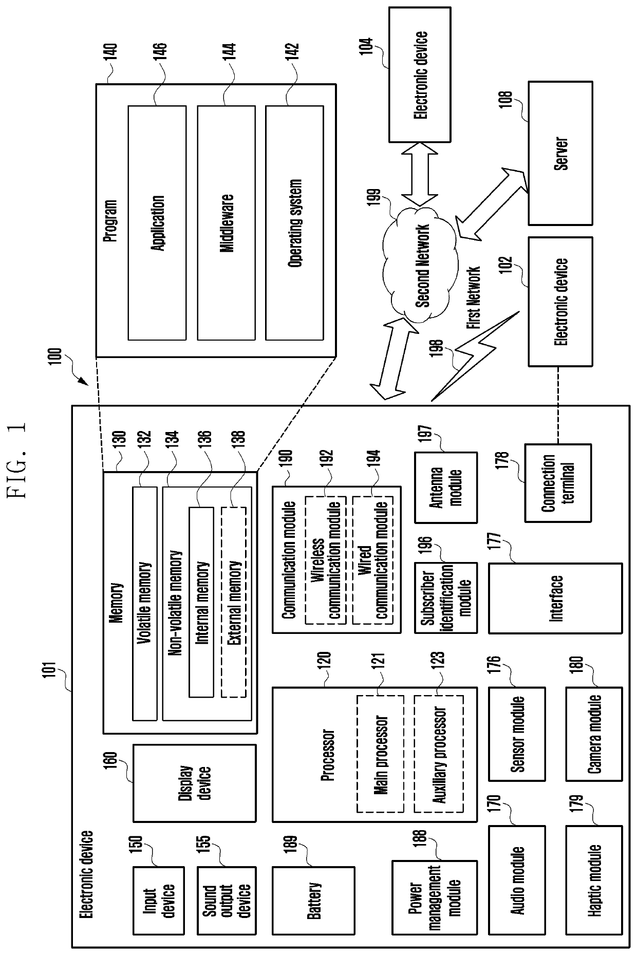
[0026]The following description with reference to the accompanying drawings is provided to assist in a comprehensive understanding of various embodiments of the disclosure as defined by the claims and their equivalents. It includes various specific details to assist in that understanding but these are to be regarded as merely exemplary. Accordingly, those of ordinary skill in the art will recognize that various changes and modifications of the various embodiments described herein can be made without departing from the scope and spirit of the disclosure. In addition, descriptions of well-known functions and constructions may be omitted for clarity and conciseness.

[0027]The terms and words used in the following description and claims are not limited to the bibliographical meanings, but, are merely used by the inventor to enable a clear and consistent understanding of the disclosure. Accordingly, it should be apparent to those skilled in the art that the following description of variou...


PUM

PropertyMeasurementUnit
thicknessaaaaaaaaaa
densityaaaaaaaaaa
thicknessaaaaaaaaaa

Abstract

A shielding member is provided. The shielding member includes a shielding layer having flexibility, and an insulating layer stacked on the shielding layer. The shielding layer includes a nanofiber layer including nanofibers plated to have electrical conductivity and coated with an adhesive material, and conductive particles disposed in the nanofiber layer.

Description

CROSS-REFERENCE TO RELATED APPLICATION(S)[0001]This application is based on and claims priority under 35 U.S.C. § 119(a) of a Korean patent application number 10-2019-0091270, filed on Jul. 26, 2019, in the Korean Intellectual Property Office, the disclosure of which is incorporated by reference herein in its entirety.BACKGROUND1. Field[0002]The disclosure relates to a shielding member performing an electromagnetic interference (EMI) shielding function and an electronic device including the same.2. Description of Related Art[0003]Electronic devices, such as a smart phone, a tablet personal computer (PC), and a laptop computer are becoming smaller, slimmer, and multifunctional. In addition, various kinds of electronic components used in such electronic devices are becoming highly integrated and having an increased speed of signal processing.[0004]When the electronic components perform signal processing, unwanted noise in the form of electromagnetic waves is generated. In the highly i...

Claims


Application Information

Patent Timeline
Patent Type & Authority Patents(United States)
IPC IPC(8): H05K9/00H05K1/18H05K1/02
CPCH05K9/009H05K1/0216H05K1/181H05K2201/093H05K9/0088H05K7/20445H05K9/0031H05K9/0083H05K1/0218
Inventor KIM, JUNGHWANLIM, JAEDEOKPARK, HYEIN
Owner SAMSUNG ELECTRONICS CO LTD
Why Eureka
Try Eureka