Optically gated transistor selector for variable resistive memory device

a variable resistive memory and selector device technology, applied in the field of programming memory devices, can solve the problems of difficult use of variable resistive memory devices, diodes that do not operate bidirectionally, and diodes that cannot properly function as selector devices for arrays of bipolar memristors, so as to reduce light intensity

Active Publication Date: 2022-04-26
BOISE STATE UNIVERSITY
View PDF33 Cites 0 Cited by
  • Summary
  • Abstract
  • Description
  • Claims
  • Application Information

AI Technical Summary

Problems solved by technology

The use of variable resistive memory devices has been difficult due the variable resistive nature of the memory devices.
However, a diode does not operate bidirectionally.
Thus, a diode selector device would not properly function as a selector device for an array of bipolar memristors.
Potentially, two opposite facing diodes in parallel could provide bidirectional functionally but may be undesirable due to added real estate on a chip as well as other fabrication complexities.
The drain-source on resistance may be problematic in using a MOSFET as a selector device for various resistance memory devices.
These sneak path currents may cause a false reading of the state of the addressed memristor.
Since the resistance variable memory element may have different resistances the voltage drop across the resistance may vary, thus changing the programming conditions to unknown conditions and limiting or preventing control of the programmed resistance state.
For example, a typical programming voltage may not be high enough to raise the resistance of the memristor to a desired state.

Method used


Image

  • Optically gated transistor selector for variable resistive memory device
  • Optically gated transistor selector for variable resistive memory device
  • Optically gated transistor selector for variable resistive memory device

Examples


Embodiment Construction

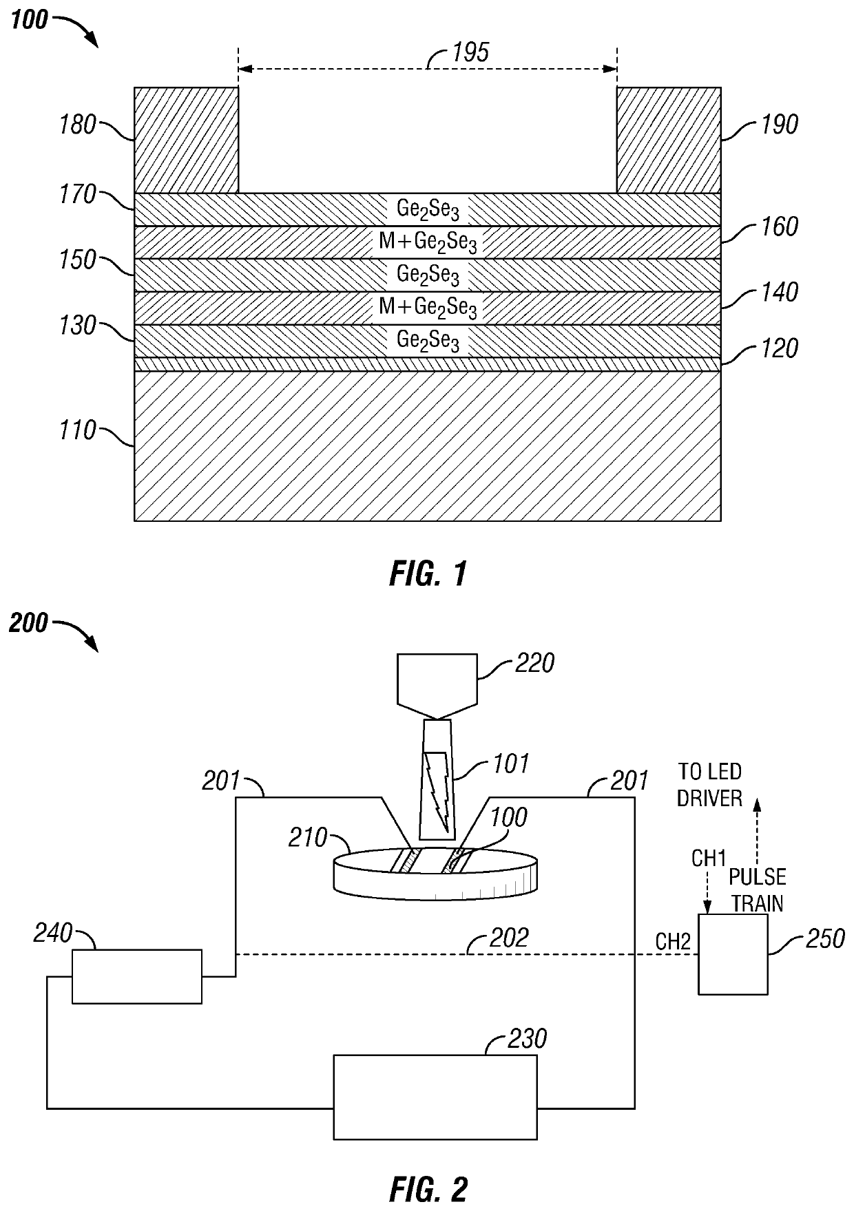
[0034]A selector device suitable for use with an array comprised of variable resistive memory devices, such as memristors, may be an OGT device as disclosed in U.S. Provisional Patent Application No. 62 / 511,119 entitled Optically Activated Transistor, Switch, and Photodiode filed on May 25, 2017 and U.S. patent application Ser. No. 15 / 990,067 entitled Optically Activated Transistor, Switch, and Photodiode filed on May 25, 2018, both which are herein incorporated by reference. An OGT device may control memristor element, or the like, programming through a combination of voltage and current, where the current is proportional to the intensity and wavelength of light applied to the gate. Operation of the OGT device is in an “enhancement” mode, whereby drain to source current may increase as a function of light intensity. To program the memristor, the OGT device may be operated in saturation, rather than between the active and cutoff modes typically used for a MOSFET transistor switch. T...


PUM

PropertyMeasurementUnit
thicknessaaaaaaaaaa
thicknessaaaaaaaaaa
thicknessaaaaaaaaaa

Abstract

An optically gated transistor (OGT) device that may be used as a selector device for one or more variable resistive memory devices. The OGT device isolates the one or more variable resistive memory devices when the OGT is not optically activated. The amount of current conducted by the OGT device is dependent on an intensity of light optically applied to the OGT device. The OGT device includes alternating layers of germanium selenide (GeSe) and GeSe plus an additional element deposited on a substrate. The OGT device includes only two electrodes connected to the alternating layers deposited on the substrate. The OGT device may generate an amplified electrical signal with respect to the magnitude of a received optical signal. The OGT device may be used to generate an optical signal having a different wavelength than the wavelength of a received optical signal.

Description

RELATED APPLICATIONS[0001]This application claims priority to and the benefit of U.S. Provisional Patent Application Ser. No. 62 / 701,335 filed on Jul. 20, 2018, and entitled “Application of optically-gated transistor as a memristor selector switch,” the contents of which are hereby incorporated by reference herein in its entirety. The application is a continuation-in-part patent application of U.S. patent application Ser. No. 15 / 990,067 filed on May 25, 2018, and entitled “Optically Activated Transistor, Switch, and Photodiode,” the contents of which are hereby incorporated by reference herein in its entirety.GOVERNMENT LICENSE RIGHTS[0002]The invention disclosed herein was funded in-part or in-whole by the U.S. Air Force Research Laboratory under Contract No. FA8750-16-C-0183. The government has certain rights in the invention disclosed herein.FIELD OF THE DISCLOSURE[0003]The embodiments described herein relate programming memory devices with apparatuses that conduct current bi-dir...

Claims


Application Information

Patent Timeline
Patent Type & Authority Patents(United States)
IPC IPC(8): H01L31/043H03F3/08H01L31/103H01L31/032H01L31/0224H01L31/0216H01L27/24H01L31/147G11C13/00
CPCH03F3/08G11C13/0069H01L27/2409H01L31/02161H01L31/022408H01L31/0324H01L31/1037H01L31/147G11C2213/72H01L31/108G11C13/003G11C2013/0088G11C13/047G11C2213/76H10B63/20H10B63/80
Inventor CAMPBELL, KRISTY A.
Owner BOISE STATE UNIVERSITY
Why Eureka
Try Eureka