
IC design data base generating method, IC design method, and electronic device using the methods

a technology of generating method and data base, applied in the direction of electric digital data processing, instruments, computing, etc., can solve the problems of design process, limited delay value information, and long design process of conventional ic (integrated circuit) design flow

Active Publication Date: 2022-04-26
REALTEK SEMICON CORP
View PDF6 Cites 0 Cited by
  • Summary
  • Abstract
  • Description
  • Claims
  • Application Information

AI Technical Summary

Benefits of technology

The patent aims to provide a method for generating a delay value database with sufficient information. It also aims to provide a method for designing an IC that refers to such a database. The technical effect of this patent is to improve the efficiency and accuracy of IC design.

Problems solved by technology

The conventional IC (Integrated Circuit) design flow needs a long time to complete the entire process.
However, the delay value of the cell in the IC to the signal may have different values in different situations, but the database used in the existing IC design flow only records the delay information of each cell under a specific application condition, thus have limited delay value information.
Such limited delay value information is not enough for the calculation of desired parameter variation results in the design process.
If the IC cell produced finally does not meet the requirements, the IC must be redesigned, that is, all design processes must be re-executed, which is a considerable burden for the relevant staff.

Method used


Image

  • IC design data base generating method, IC design method, and electronic device using the methods
  • IC design data base generating method, IC design method, and electronic device using the methods
  • IC design data base generating method, IC design method, and electronic device using the methods

Examples


Embodiment Construction

[0017]In following descriptions, a plurality of embodiments are provided to explain the concept of the present invention. Please note, each of following embodiments can be implemented by hardware (e.g. circuit or device), and can be implemented by firmware (e.g. a processor installed with at least one program).

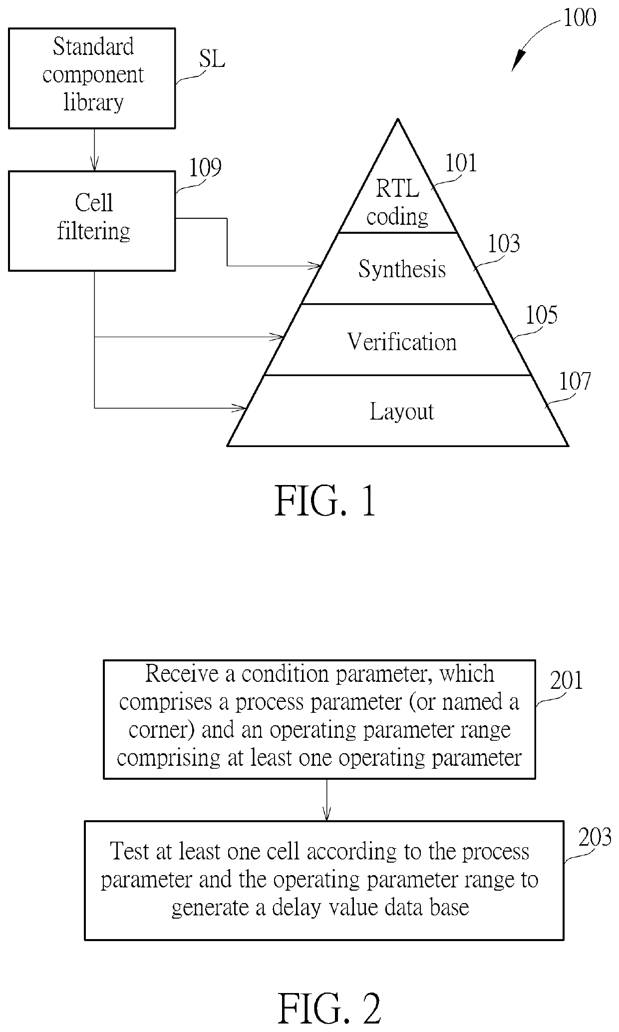
[0018]FIG. 1 is a schematic diagram illustrating an IC design flow according to one embodiment of the present invention. As shown in FIG. 1, the IC design flow 100 comprises steps of RTL coding 101, synthesis 103, verification 105 (e.g. static timing analysis, STA), and layout 107. In RTL coding 101, the module function is described by codes by hardware description languages such as VHDL, Verilog). That is, the actual hardware circuit function is described by HDL languages to form RTL (register-transfer level) codes. In synthesis 103, the RTL codes are converted to a file format describing the circuit (e.g. netlist). In verification 105, the timing or function of the circuit i...


PUM


Abstract

An IC design data base generating method, including: receiving a condition parameter, which comprises a process parameter and an operating parameter range comprising at least one operating parameter; and testing at least one cell according to the process parameter and the operating parameter range to generate a delay value data base. The delay value data base comprises a plurality of delay values, wherein the plurality of delay values for an identical cell correspond to the operating parameter range with an identical type but different value. An IC design method using the delay value data base is also disclosed.

Description

BACKGROUND OF THE INVENTION1. Field of the Invention[0001]The present invention relates to an IC design data base generating method, an IC design method and an electronic device using the methods, and particularly relates to an IC design data base generating method and an IC design method which can provide cell delay value information and an electronic device using the methods.2. Description of the Prior Art[0002]The conventional IC (Integrated Circuit) design flow needs a long time to complete the entire process. However, the delay value of the cell in the IC to the signal may have different values in different situations, but the database used in the existing IC design flow only records the delay information of each cell under a specific application condition, thus have limited delay value information. Such limited delay value information is not enough for the calculation of desired parameter variation results in the design process. Therefore, the IC only can be tested to determin...

Claims


Application Information

Patent Timeline
Patent Type & Authority Patents(United States)
IPC IPC(8): G06F30/30G06F30/337G06F30/327G06F119/06G06F119/08
CPCG06F30/337G06F30/327G06F2119/06G06F2119/08G06F30/3312G06F30/392G06F2119/12
Inventor HUANG, SZU-YINGYU, MEI-LILO, YU-LANKAO, SHU-YI
Owner REALTEK SEMICON CORP
Learn More