Smart wearable device

a wearable device and smart technology, applied in the field of wearable devices, can solve the problems of device failure, limited aesthetic design options, microstrip patch antennas are inherently narrowband, etc., and achieve the effect of defining the operating bandwidth and efficiency of the devi

Active Publication Date: 2022-02-22
SMARTLINE BV
View PDF7 Cites 0 Cited by
  • Summary
  • Abstract
  • Description
  • Claims
  • Application Information

AI Technical Summary

Benefits of technology

[0007]In order to achieve said object of the invention, a wearable device of the type as described in the opening paragraph, according to the present invention, is characterized in that said outer shell comprises a first shell part that defines a first circumference of the device and comprises said first surface, in that said outer shell comprises a second shell part that defines a second circumference of the device and comprises said second surface, in that said first shell part and said second shell part are formed at least substantially of metal and are at least partially separated from one another by said dielectric, in that said first shell part forms said patch conductor at said first exposed surface, in that said second shell part forms said ground conductor at said second exposed surface, and in that said first shell part and said second shell part together form said patch antenna. Hence, according to the invention, the metallic shell parts of the wearable device that are exposed to the external environment do not require any additional enclosure or insulation around them and are essentially used as active components of the antenna. This provides a relatively large or even maximum radiating surface area of the patch that, together with required dielectric separation between patch and ground conductors, defines the operating bandwidth and efficiency of the device.
[0009]The invention solves the aesthetical and performance problems of the known antenna in a metal shell by maximizing the metal surface of the top of the piece of jewel by essentially converting the top metal surface of this jewel into compact patch microstrip (PIFA) antenna that is directly exposed to the environment. The performance of this antenna is practically as good as can be theoretically achieved from the given overall sizes of the structure that particularly constitutes a piece of jewel. This includes the operating bandwidth in which the antenna is well matched to its feeder and provides a stable radiation pattern combined with a high efficiency. Since there is no requirement for an insulation or other protective enclosure covering the metal shell parts, the invention allows more freedom of the design of the jewel's metal surface, which makes the smart jewel more attractive, by enabling a precious-metal and jewellery look and feel. The design also yields more possibilities for the placement of components inside the jewel because there is no need for clearance zones on a printed-circuit board (PCB), in contrast to the requirements imposed, for example, by conventional chip antennas which, essentially, make the PCB behave as a crucial part of the antenna. The patch conductor may be mechanically stabilized by a dielectric support, which is visible from outside the jewel, but which is seamlessly incorporated into the aesthetic design of the jewel.
[0012]A compact microstrip patch antenna can be achieved by grounding the patch conductor at one end, such that the patch conductor and the ground conductor form a quarter-wave resonator at the operating frequency, thus reducing the size of the antenna. To this end, a further embodiment of the device according to the invention is characterized in that said core comprises at least one shortening spring or pin or other electromechanical connector that is configured to connect said patch conductor to said ground conductor. In a further embodiment, shortening spring(s) are connected to printed-circuit board (PCB) acting as ground layer, which in turn is connected to the bottom metal shell part of the device acting as a ground conductor.
[0016]The top patch conductor of the exposed antenna, the bottom ground conductor, and the dielectric (insulation) between the top and the bottom of the device are adjusted to balance the desired aesthetics and a good performance. The antenna may be tuned by repositioning of grounding springs and a feeder spring inside the smart jewel. To that end, a further specific embodiment of the device according to the invention is characterized in that at least one of said at least one feeder spring and at least one shorting spring is adjustable, particularly displaceable, for fine tuning of said patch antenna. Alternatively, or additionally, a further specific embodiment of the device according to the invention is characterized in that said patch antenna is tuned by an electronic circuitry arrangement.
[0019]In order to add to the look and feel of the device as a jewel, while providing improved antenna functionality, such wearable device according to the invention is characterized in that said first and said second shell part constitute said patch conductor and said ground conductor respectively and are made of metal, particularly of at least one precious metal, and more particularly of at least one noble metal. To further give the device a more luxurious appearance, a further embodiment thereof is characterized in that at least said first shell part is set with at least one jewel from a group containing crystals, semi-precious stones and gemstones, and / or ceramic or other decorative inserts.

Problems solved by technology

However, due to the small distance between the patch conductor and the ground conductor, microstrip patch antennas are inherently narrowband.
This approach, however, limits aesthetic design options and device would not be considered a jewel as it wouldn't have metallic look and feel.
In addition, such design may reduce the performance of antenna, resulting in a reduced range, narrow band, and / or a lossy antenna.

Method used


Image

  • Smart wearable device
  • Smart wearable device
  • Smart wearable device

Examples


Embodiment Construction

[0030]Example embodiments will now be described more fully with reference to the accompanying drawings.

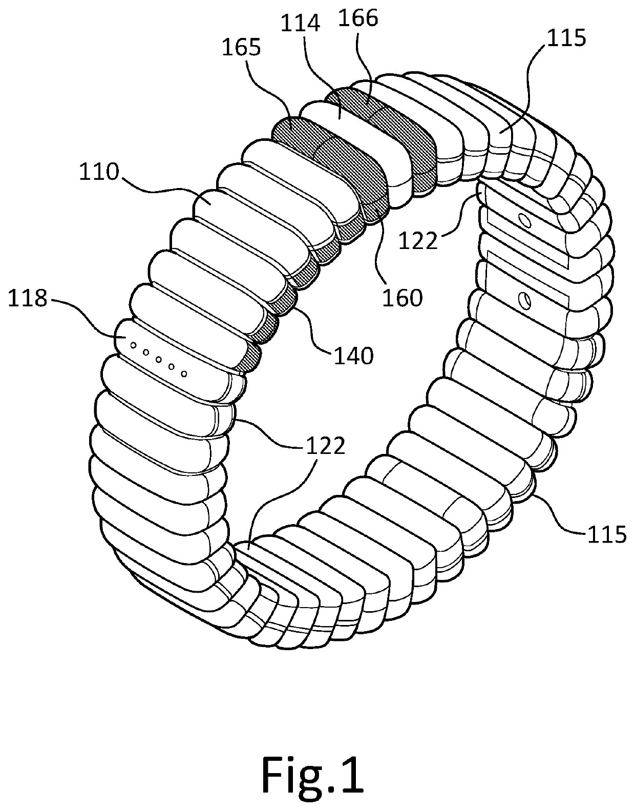
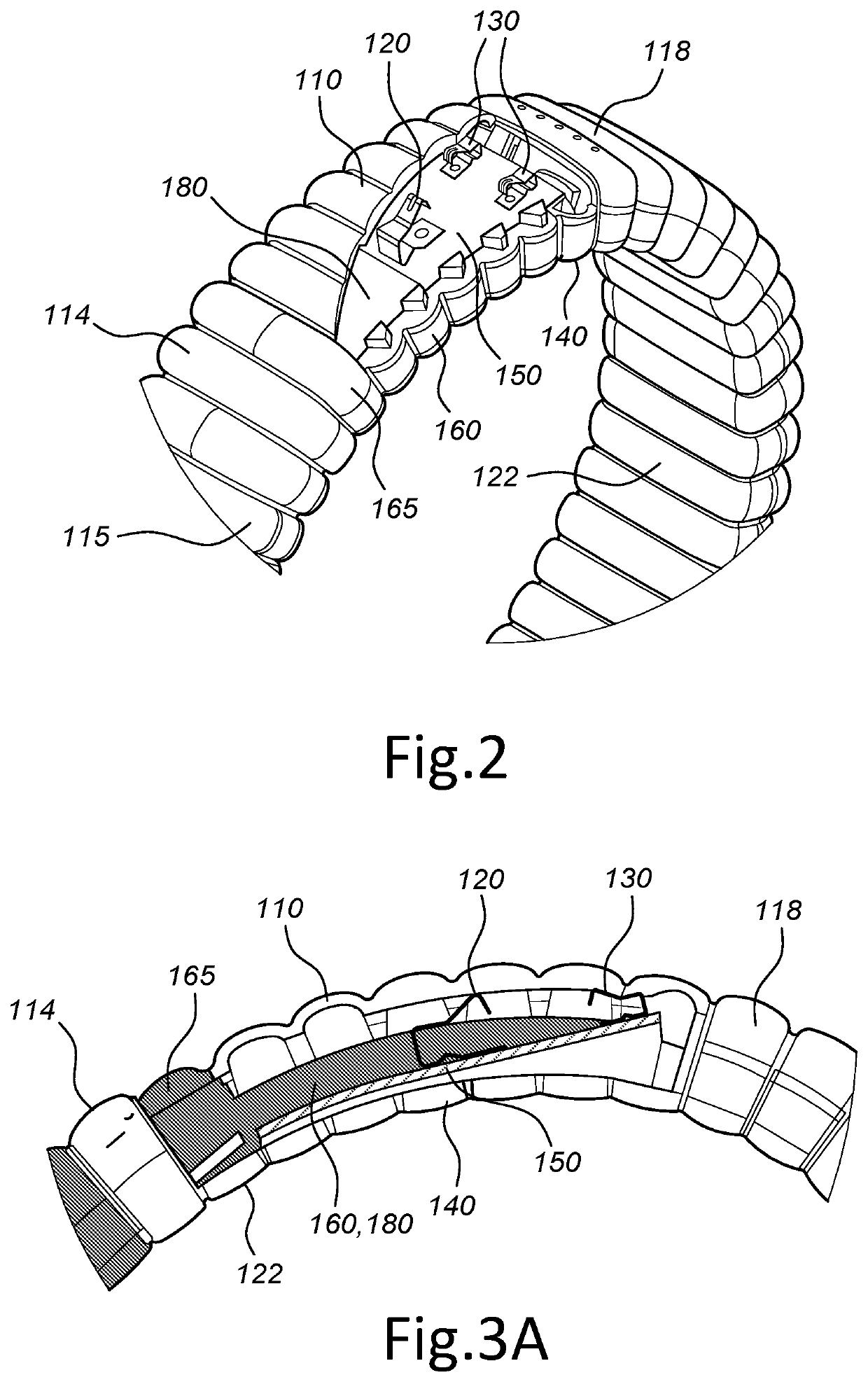
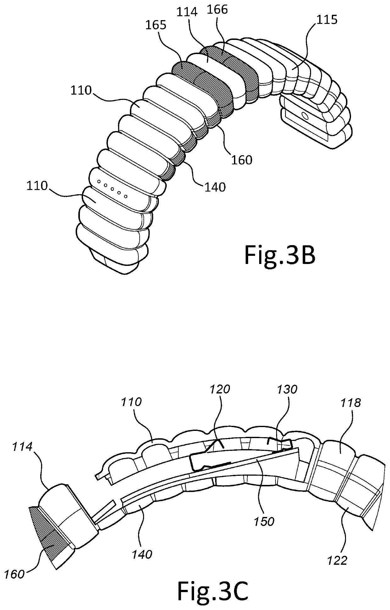
[0031]FIG. 1 illustrates a perspective view of a device according to an embodiment of the present invention. The device basically consists of a structure that is configured and shaped to be worn by a user. In an embodiment, this structure is a wearable device such as smart jewellery and, for example, forms a bracelet, flat connected pendants, ring, necklace and the like, capable of being used for wireless communication. The device may include both metal and non-metal components. The surface may have any 3-D design / pattern such as a zigzag pattern, wave like-design and the like. In one embodiment, the device includes an exposed (first) top surface 118 and an exposed (second) bottom surface 122, such that the top surface 118 includes a patch conductor 110 and the bottom surface 122 includes a ground conductor 140. The device further comprises a hollow core formed between the top surf...


PUM


Abstract

A wearable device comprises wireless communication means and a patch antenna that is coupled to said wireless communication means to receive and / or transmit electromagnetic radiation. Said patch antenna comprises a planar patch conductor and a planar ground conductor that are separated by a dielectric in between said patch conductor and said ground conductor while at least partially overlapping with one another. The device comprises a core inside a shell and comprises at least part of said communication means within said core. Said shell comprises a first shell part and a second shell part opposite said first shell part, wherein said first shell part and said second shell part are at least partially separated by said dielectric. Said first shell part comprises said patch conductor and said second shell part comprises said ground conductor. Said first shell part and said second shell part together form said patch antenna. The wearable device particularly is a piece of jewellery.

Description

CROSS REFERENCE TO RELATED APPLICATIONS[0001]This application is a national stage filing of PCT International Application No. PCT / NL2019 / 050007, filed Jan. 7, 2019, which is based on and claims priority to Netherlands Patent Application No. 2020241, filed Jan. 5, 2018.FIELD OF THE INVENTION[0002]The present invention relates to a wearable device, comprising a structure that is configured to be worn by a user, said structure having a first exposed surface and a second exposed surface, said second surface being located closer to the user than said first surface when the structure is being worn by the user, said structure comprising wireless communication means and comprising a patch antenna that is coupled to said wireless communication means to receive and / or transmit electromagnetic radiation, wherein said patch antenna comprises a substantially planar patch conductor and a substantially planar ground conductor that are separated by a dielectric in between said patch conductor and s...

Claims


Application Information

Patent Timeline
Patent Type & Authority Patents(United States)
IPC IPC(8): H01Q3/44H01Q9/04H01Q1/27H04B1/3827H01Q1/24H01Q9/16H01Q1/52
CPCH01Q9/0421H01Q1/273H04B1/385H01Q1/243H01Q1/528H01Q9/04H01Q9/16H01Q1/44
Inventor POLTAVTSEV, DMYTRO BORYSOVYTCH
Owner SMARTLINE BV
Why Eureka
Try Eureka