Method of forming a pattern and method of manufacturing a semiconductor device using the same

a technology of pattern and semiconductor, which is applied in the direction of semiconductor devices, electrical devices, transistors, etc., can solve the problems of reducing and achieve the effect of preventing the deterioration of the reliability of the semiconductor device due to the electrical short between the landing pads

Active Publication Date: 2021-06-22
SAMSUNG ELECTRONICS CO LTD
View PDF16 Cites 0 Cited by
  • Summary
  • Abstract
  • Description
  • Claims
  • Application Information

AI Technical Summary

Benefits of technology

[0007]In a method of manufacturing a semiconductor device, by performing a trimming process on a mask for forming landing pads, a major axis and a minor axis of the mask is adjusted. Accordingly, the deterioration of the reliability of the semiconductor device due to the electrical short between the landing pads may be prevented.

Problems solved by technology

However, as the degree of integration of the semiconductor device increases, the landing pads are formed with less of a process margin, and the reliability of the semiconductor device may be reduced.

Method used


Image

  • Method of forming a pattern and method of manufacturing a semiconductor device using the same
  • Method of forming a pattern and method of manufacturing a semiconductor device using the same
  • Method of forming a pattern and method of manufacturing a semiconductor device using the same

Examples


Embodiment Construction

[0010]A method of forming a pattern and a method of manufacturing a semiconductor device using the same in accordance with example embodiments will be described more fully hereinafter with reference to the accompanying drawings.

[0011]Hereinafter, two directions intersecting with each other among horizontal directions substantially parallel to an upper surface of a substrate are defined as first and second directions, respectively, and a vertical direction substantially perpendicular to the upper surface of the substrate is defined as a third direction. In example embodiments, the first and second directions may be orthogonal to each other.

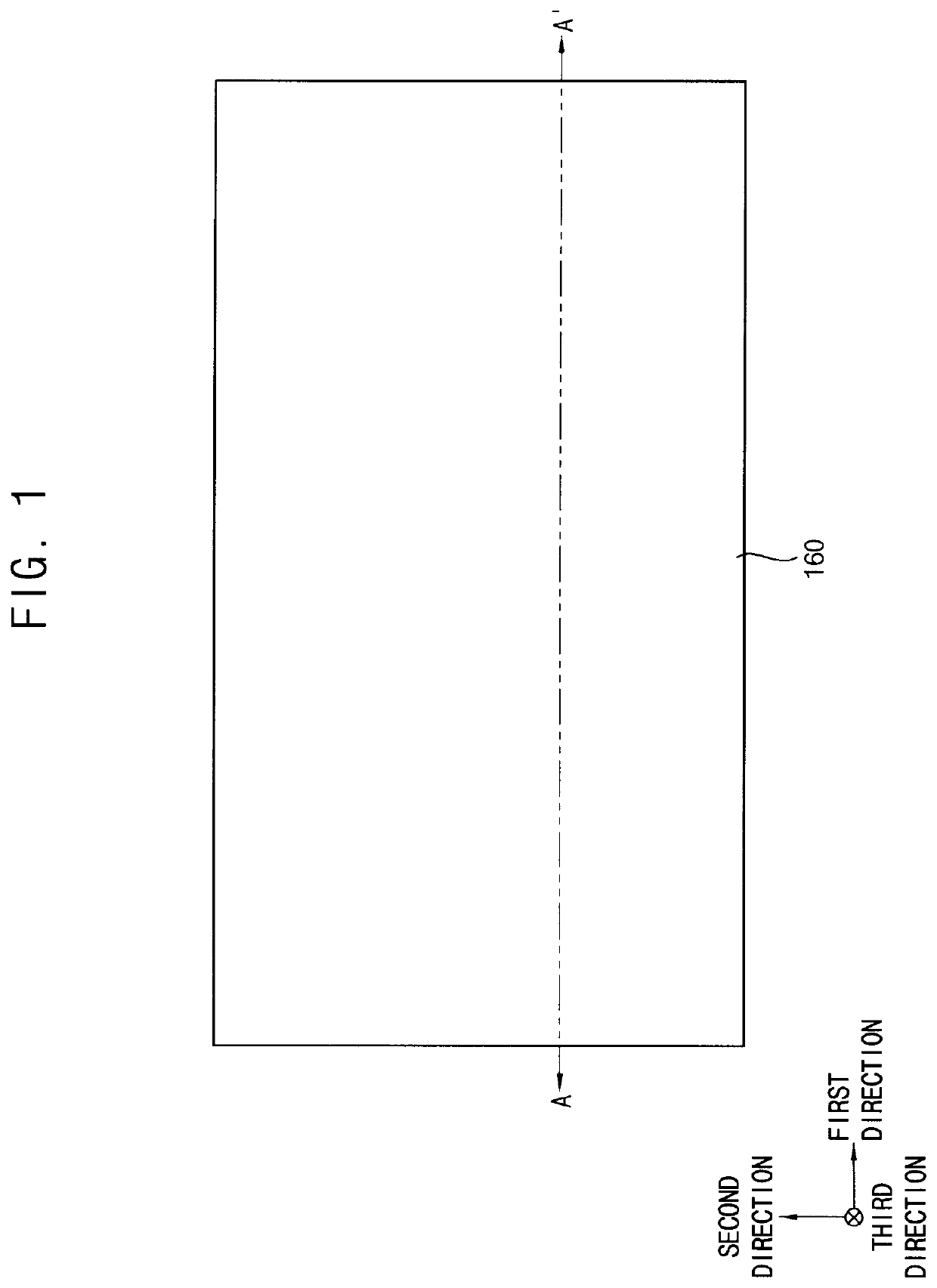
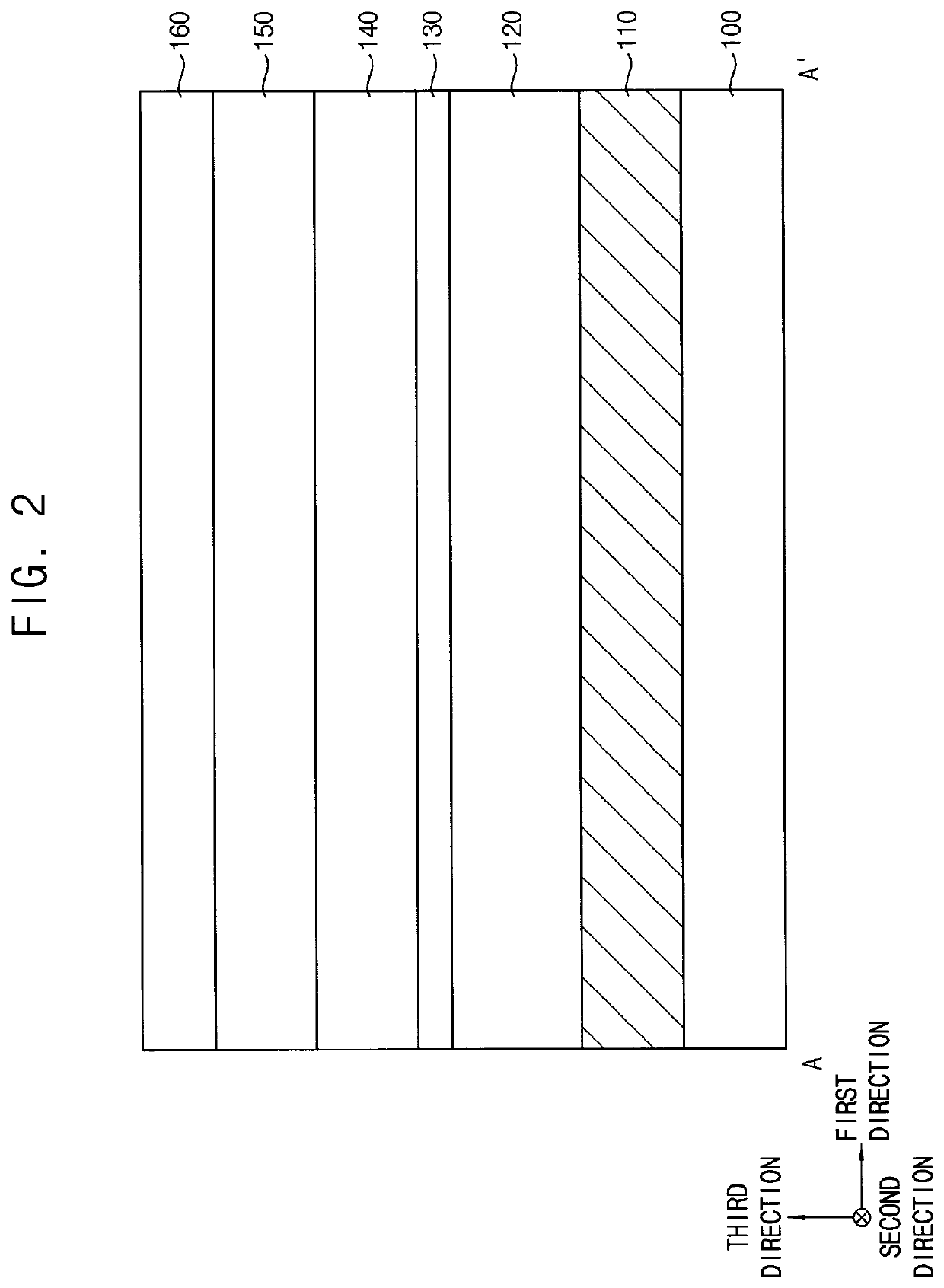
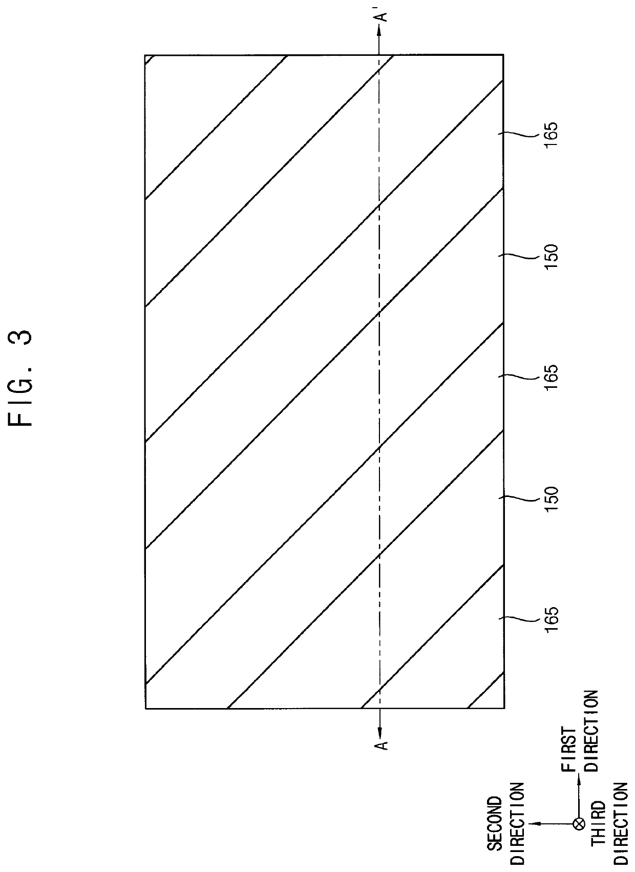
[0012]FIGS. 1 to 31 are plan views, cross-sectional views and perspective views illustrating a method of forming a pattern in accordance with example embodiments. Specifically, FIGS. 1, 3, 7, 13, 15, 17, 19, 24A, 24B, 26, 28 and 30 are the plan views, FIGS. 2, 4-6, 8-12, 16, 18 and 20-23 are the cross-sectional views, and FIGS. 14, 25, 27, 29 and 3...


PUM

PropertyMeasurementUnit
aspect ratioaaaaaaaaaa

Abstract

First and second mask layers are formed on a target layer. The second mask layer is patterned to form second mask patterns each of which having a rhomboid shape with a first diagonal length and a second diagonal length. A trimming process is performed on the second mask patterns to form second masks by etch. First portions of first opposite vertices of each second mask pattern are etched more than second portions of second opposite vertices of each second mask pattern. A first diagonal length between the first opposite vertices is greater than a second diagonal length between the second opposite vertices. The first mask layer is patterned to form first masks by etching the first mask layer using the second masks as an etching mask. The target layer is patterned to form target patterns by etching the target layer using the first masks as an etching mask.

Description

CROSS-REFERENCE TO RELATED APPLICATION[0001]This application claims priority under 35 USC § 119 to Korean Patent Application No. 10-2019-0001697 filed on Jan. 7, 2019 in the Korean Intellectual Property Office (KIPO), the contents of which are herein incorporated by reference in their entirety.BACKGROUND1. Field[0002]Example embodiments relate to a method of forming a pattern and a method of manufacturing a semiconductor device using the same.2. Description of the Related Art[0003]In manufacturing semiconductor devices, bit lines and conductive layers with landing pads between the bit lines may be formed on a substrate. However, as the degree of integration of the semiconductor device increases, the landing pads are formed with less of a process margin, and the reliability of the semiconductor device may be reduced.SUMMARY[0004]According to an exemplary embodiment of the present inventive concept, a method of forming a pattern is provided. A first mask layer is formed on a target la...

Claims


Application Information

Patent Timeline
Patent Type & Authority Patents(United States)
IPC IPC(8): H01L21/3213H01L27/108H01L21/033
CPCH01L21/32139H01L21/0332H01L21/0334H01L21/0337H01L27/10855H01L27/10885H10B12/0335H10B12/482H01L21/0338H01L21/76816
Inventor LEE, MYEONG-DONGCHOI, MIN-SUAHN, JUN-HYEOKHAN, SUNG-HEEHONG, CE-RA
Owner SAMSUNG ELECTRONICS CO LTD
Why Eureka
Try Eureka