Integrated memory device and method of operating same

a memory device and integrated circuit technology, applied in information storage, static storage, digital storage, etc., can solve the problems of limiting the ability of these sense amplifiers to reliably detect very small signal differences on bit lines, limiting the smallest memory cell size, and limiting so as to improve the read signal margin, and reliably sense small voltage excursions on bit lines

Active Publication Date: 2021-05-04
CELIS SEMICONDUCTOR CORP
View PDF13 Cites 0 Cited by
  • Summary
  • Abstract
  • Description
  • Claims
  • Application Information

AI Technical Summary

Benefits of technology

[0024]In light of the foregoing, it is an object of this invention to provide a new read method that increases the read signal margin by adding an additional step to the read cycle where additional charge is applied to the bit lines between the two steps of precharging the bit lines and transferring charge between the bit lines and the memory cells. It is another object of this invention to use this new read method for memories that use charge storage capacitors by using a memory circuit configuration that does not use floating bit lines during a portion or all of the sensing part of the read cycle to improve read signal margin. It is another object of this invention to use the new read method by providing a preamplifier that nulls out its voltage offset and operates with non-floating bit lines to reliably sense small voltage excursions on bit lines, improving read signal margin. It is another object of this invention to allow a smaller memory storage device, resulting in a denser memory configuration that provides for more memory capacity on a silicon chip and reducing the cost per bit. It is another object of this invention to use the new read method to provide an FRAM with a reduced read voltage for higher endurance nonvolatile memory applications. It is another object of this invention to use the new read method to provide a reference memory cell that provides a reliable reference for a 1T / 1C FRAM memory cell configuration. It is further object of this invention to use the new read method to provide a reference memory cell that provides a reliable reference for a DRAM memory cell configuration.
[0025]These and other objects, features and advantages are provided according to the current invention by integrated circuit memory devices and methods in which higher capacity, lower cost per bit and more reliable semiconductor memories can be manufactured.
[0026]The current invention provides an integrated circuit preamplifier with a self-nulling feature and associated reference circuits that eliminate offset of the preamplifier allowing the preamplifier to sense small read signal voltage differentials on non-floating bit lines. This self-nulling preamplifier circuit can be used in reading data states in almost any type of integrated circuit memory where small signals on bit lines need to be detected.
[0027]The current invention provides a method of operation where the bit lines do not float during part or all of the read sensing portion of the read cycle for integrated circuit memories that typically have used floating bit lines for the sensing portion of the read cycle. For FRAMs, use of non-floating bit lines reduces the limitation on switching voltage on the ferroelectric capacitor during the sensing portion of the read cycle while at the same time allowing the read signals to be reliably sensed. For DRAMs, use of non-floating bit lines increases the read signal margin by allowing a self-nulling preamplifier to be used that can sense small signal differentials on bit lines and overcome offsets common to latching sense amplifiers.
[0029]For a given technology node or design rule, the combined effect of these improvements can result in memory cells that require less silicon area than the prior art memory cells, improving the memory capacity for a given silicon chip area, reducing the cost per bit, providing a higher level of reliability, and allowing the memory cell to scale to smaller technology nodes.
[0031]The current invention also provides an integrated circuit memory device reference cell that operates with non-floating bit lines comprising: a pair of memory storage devices programmed to opposite data states and connected in a parallel circuit configuration at a predetermined time during the read cycle to provide a reliable reference signal for a sense amplifier.

Problems solved by technology

The problem is that the read signal margin attainable by conventional memory designs limits the minimum size memory storage device that can be used and therefore limits the smallest memory cell size.
Read signal margin is limited by two significant issues in typical memory designs.
First, because of manufacturing process variations, typical latching sense amplifier circuits that read the data states of memory cells along the bit lines have variable so-called offsets that limit the ability of these sense amplifiers to reliably detect very small signal differences on bit lines.
Secondly, when memories that store data on charge storage capacitors use floating bit lines for the sensing portion of the read cycle, a capacitor divider effect reduces the read signal margin.
However, manufacturing process variations, including reticle alignment accuracies, cause the offset to vary and limit how well these sense amplifiers can perform.
These variations can affect the circuits on different parts of the same chip of silicon as well as circuits on different chips of silicon and different manufacturing lots of silicon, providing non-uniform behavior of the sense amplifiers.
DRAMs are volatile in that the data must be refreshed in the memory at regular and short intervals (typically less than 100 millisecond refresh time) because the data are lost even if the power remains applied to the memory.
Typical DRAMs and FRAMs have read cycles that are destructive meaning that the logic state in a memory cell is lost during the read operation.
This charge sharing reduces the read signal strength obtainable on the bit line.
In the case of an FRAM, the series capacitance effect also limits the magnitude of the switching voltage that can be applied across the ferroelectric capacitor
These factors increase the cost per bit of a typical FRAM.
These latter types of memory cells are typically referred to as 1T / 1C memory cells, but the industry has had a difficult time developing a sense amplifier reference signal that allows a logic state “1” to be distinguished reliably from a logic state “0”.
This difficulty arises because of low read signal strength on the bit lines and sense amplifier offset.

Method used


Image

  • Integrated memory device and method of operating same
  • Integrated memory device and method of operating same
  • Integrated memory device and method of operating same

Examples


Embodiment Construction

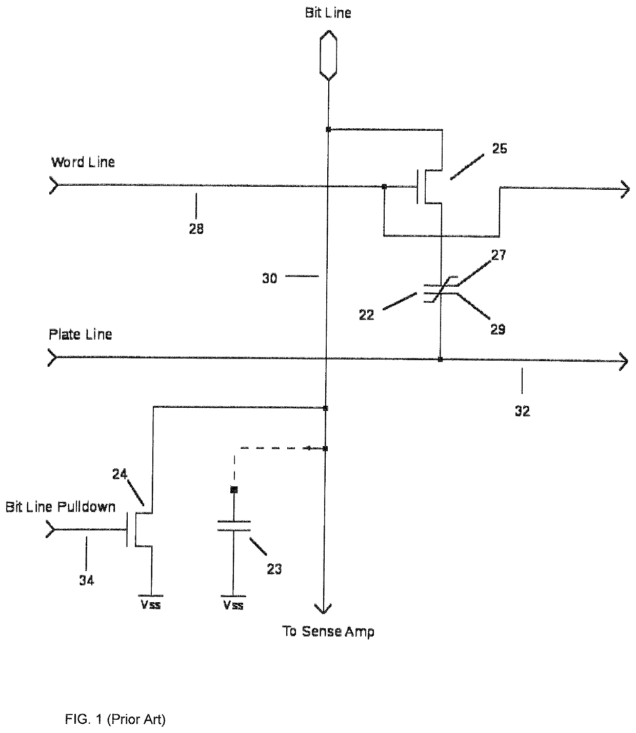
[0045]In contrast to prior art memories that have used floating bit lines, such as DRAMs and FRAMs, the preferred embodiment of the current invention (1) operates with non-floating bit lines during the sensing portion of the read cycle, (2) uses a self-nulling differential preamplifier that applies additional charge to non-floating bit lines to eliminate offset in the preamplifier so that small data signals on bit lines can be sensed, (3) uses a latching sense amplifier connected to the outputs of the preamplifier in order to latch the data, and (4) uses a reference memory cell design based on the current invention to provide a reference signal for the preamplifier.

[0046]An alternate embodiment of the current invention for an FRAM (1) operates with non-floating bit lines during the sensing portion of the read cycle, (2) applies additional charge to the bit lines during the sensing portion of the read cycle, and (3) uses a reference memory cell design based on the current invention t...


PUM


Abstract

An integrated circuit memory contains a memory cell connected to a bit line that does not float during a portion or all of the read sensing part of the read cycle. The memory cell includes a data storage device. The data storage device may be a ferroelectric capacitor, a linear capacitor, a floating gate transistor, a magnetic device, a resistive device or other type of data storage device capable of placing a charge on the bit line corresponding to a specific data state of the memory cell. The bit line and a reference bit line are connected to a differential amplifier and precharged to specified voltages. Preferably, a self-nulling sense amplifier circuit is connected to the bit lines that compensates for sense amplifier offset by applying additional charges on the bit lines. Alternatively, charge sources may be connected to the bit lines to provide additional charges on the bit lines during the read cycle. Memory cells according to this invention can be configured to provide a reference cell for the reference bit line.

Description

FIELD OF THE INVENTION[0001]The current invention relates to integrated circuit devices and methods of operation thereof, and more particularly, to integrated circuit memory devices that sense the data state of a memory cell along bit lines and methods of operation thereof, but its scope applies to any memory cells and memory arrays that may use features of this invention. A memory device may be a semiconductor memory chip, an embedded memory array or a memory macro but also could be any latches that might store data or logic states of information, among others.BACKGROUND OF THE INVENTION[0002]Integrated circuit memory devices are used to store information in a wide variety of electronic devices including, among others, personal computers, laptop computers, tablets, cellular telephones, data servers, digital cameras and video recorders. For example, an integrated circuit memory device may be used to store data for retrieval and processing by a microprocessor or similar data processi...

Claims


Application Information

Patent Timeline
Patent Type & Authority Patents(United States)
IPC IPC(8): G11C11/22
CPCG11C11/2275G11C11/2255G11C11/2273G11C11/221G11C11/409
Inventor DIETRICH, DARYL GDERBENWICK, GARY F
Owner CELIS SEMICONDUCTOR CORP
Why Eureka
Try Eureka