
Display device, method for manufacturing the device and laser processing apparatus for manufacturing the display device

a display device and laser processing technology, applied in sustainable manufacturing/processing, identification means, instruments, etc., can solve the problems of curved display panels being more susceptible to impact damage and vulnerable to impact, and achieve the effect of resisting external impa

Active Publication Date: 2021-01-26
SAMSUNG DISPLAY CO LTD
View PDF12 Cites 0 Cited by
  • Summary
  • Abstract
  • Description
  • Claims
  • Application Information

AI Technical Summary

Benefits of technology

The modified display device exhibits improved resistance to external impacts, enhancing its reliability by making the curved portions more capable of withstanding external forces, thus improving the overall durability and performance.

Problems solved by technology

However, the curved display panel may be more susceptible to impact damage as compared with a rectangular linear display panel.
Particularly, the curved display panel includes a curved portion and a linear portion according to a shape thereof, in which the linear portion generally absorbs the impact in a surface contact form at the time of external impact to disperse the impact, but the curved portion absorbs the impact in a dot contact form, and thus, may be vulnerable to the impact.

Method used


Image

  • Display device, method for manufacturing the device and laser processing apparatus for manufacturing the display device
  • Display device, method for manufacturing the device and laser processing apparatus for manufacturing the display device
  • Display device, method for manufacturing the device and laser processing apparatus for manufacturing the display device

Examples


Embodiment Construction

[0028]In the following description, for the purposes of explanation, numerous specific details are set forth in order to provide a thorough understanding of various exemplary embodiments or implementations of the invention. As used herein “embodiments” are non-limiting examples of devices or methods employing one or more of the inventive concepts disclosed herein. It is apparent, however, that various exemplary embodiments may be practiced without these specific details or with one or more equivalent arrangements. In other instances, well-known structures and devices are shown in block diagram form in order to avoid unnecessarily obscuring various exemplary embodiments. Further, various exemplary embodiments may be different, but do not have to be exclusive. For example, specific shapes, configurations, and characteristics of an exemplary embodiment may be used or implemented in another exemplary embodiment without departing from the inventive concepts.

[0029]Unless otherwise specifi...


PUM

PropertyMeasurementUnit
DAaaaaaaaaaa
area DAaaaaaaaaaa
thicknessaaaaaaaaaa

Abstract

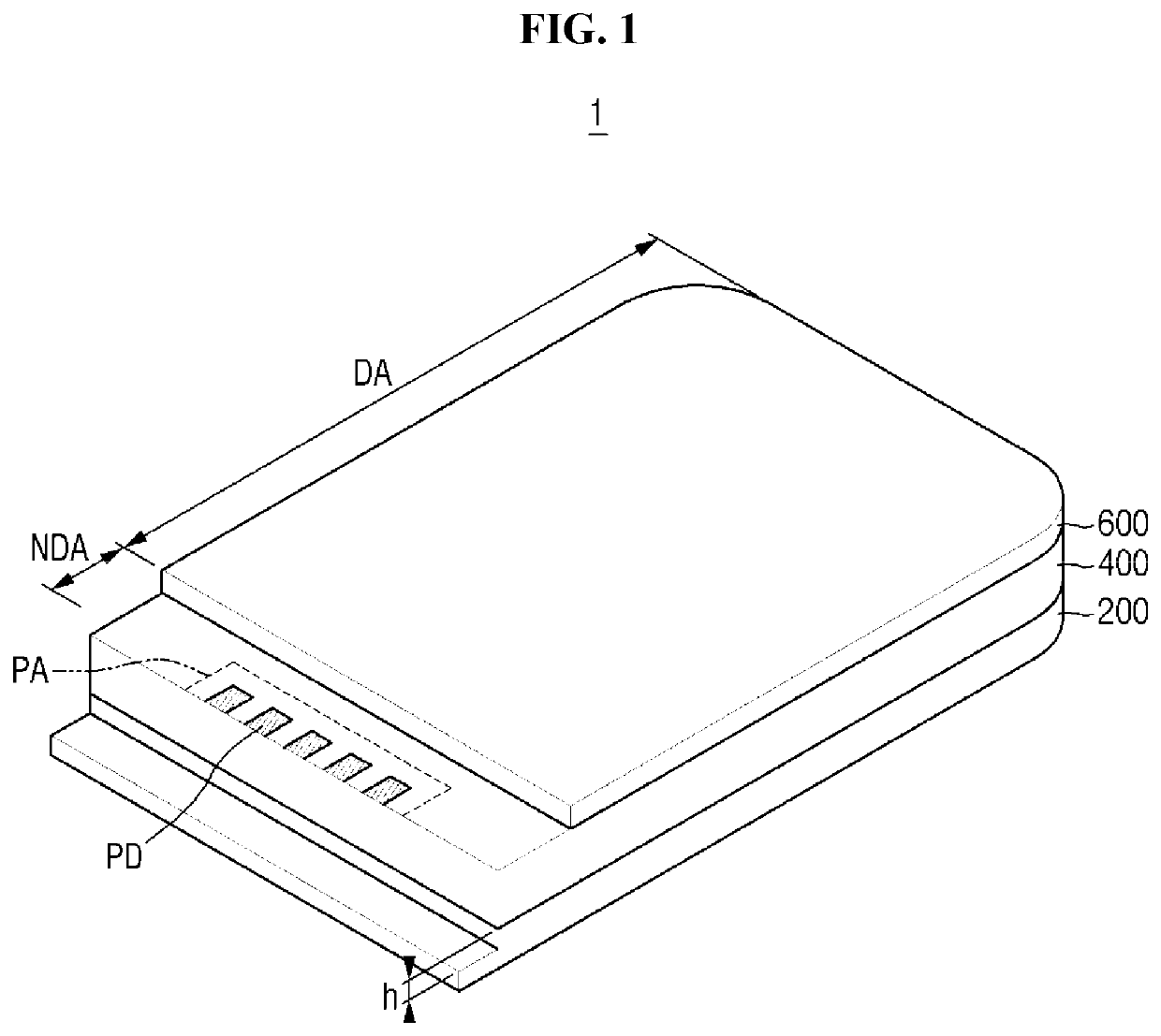
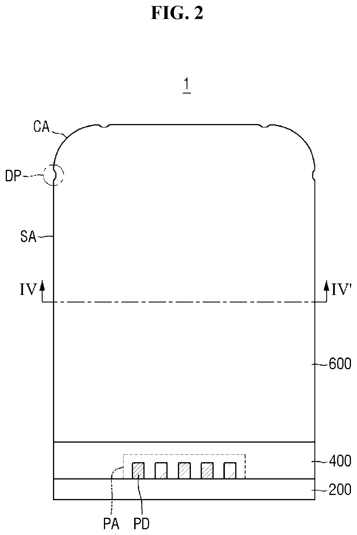
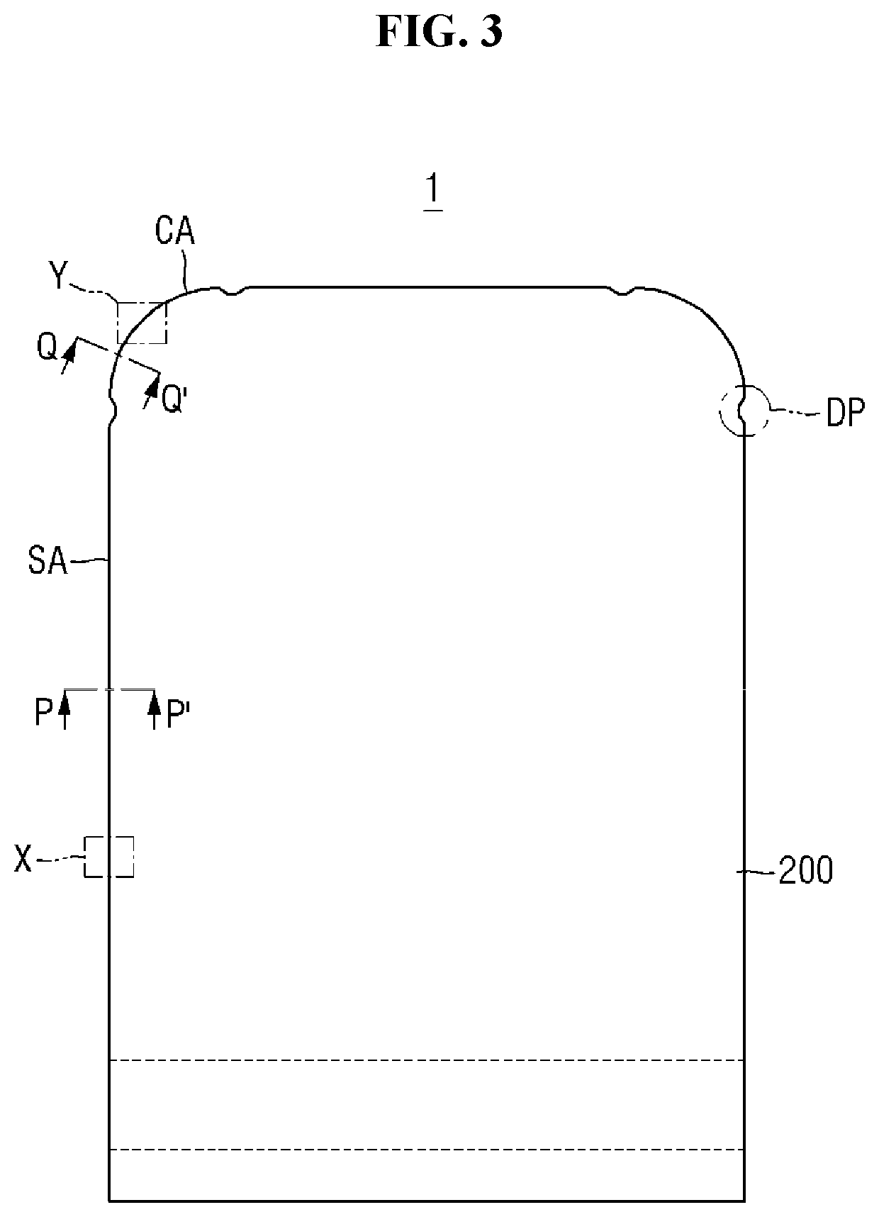
A display device including a linear portion and a curved portion, including a first substrate including a first surface and a second surface opposite the first surface; a second substrate including a third surface and a fourth surface opposite the third surface; and a display panel disposed between the first surface of the first substrate and the fourth surface of the second substrate. An outer surface adjacent to the first surface of the first substrate protrudes outward from an outer surface adjacent to the second surface of the first substrate, and a first width of a region of the first surface of the first substrate that does not overlap with the second surface in the linear portion is greater than a second width of a region of the first surface of the first substrate that does not overlap with the second surface of the first substrate in the curved portion.

Description

CROSS-REFERENCE TO RELATED APPLICATION[0001]This application claims priority from and the benefit of Korean Patent Application No. 10-2018-0061012, filed on May 29, 2018, which is hereby incorporated by reference for all purposes as if fully set forth herein.BACKGROUNDField[0002]Exemplary embodiments of the invention relate generally to a display device, a method for manufacturing the display device, and a laser processing apparatus for manufacturing the display device.Discussion of the Background[0003]A display device used for displaying an image typically includes a display panel, such as an organic light emitting display panel or a liquid crystal display panel. With development of technology, there is an increasing demand for a display panel with a large display area and a display panel having a curved surface. However, the curved display panel may be more susceptible to impact damage as compared with a rectangular linear display panel.[0004]Particularly, the curved display panel...

Claims


Application Information

Patent Timeline
Patent Type & Authority Patents(United States)
IPC IPC(8): H01L21/00G06F1/16F21V8/00G02B5/30H01L51/00H10K99/00
CPCG06F1/1652G02B5/3025G02B6/0056H01L51/0097G09F9/30H10K59/12H10K59/1201G02B27/286G06F1/1626Y02E10/549Y02P70/50H10K77/10B23K26/073H10K77/111
Inventor YUG, GEUN WOOKANG, KU HYUN
Owner SAMSUNG DISPLAY CO LTD
Learn More