
Display panel and electronic device including the same

a technology of electronic devices and display panels, applied in the direction of semiconductor devices, photovoltaic energy generation, electrical apparatus, etc., can solve the problems of easy damage of organic light emitting elements, easy moisture or oxygen exposure, etc., and achieve the effect of improving reliability and lifetime, and avoiding damag

Active Publication Date: 2020-06-02
SAMSUNG DISPLAY CO LTD
View PDF12 Cites 9 Cited by
  • Summary
  • Abstract
  • Description
  • Claims
  • Application Information

AI Technical Summary

Benefits of technology

[0004]An organic light emitting display panel includes an organic light emitting element. The organic light emitting element may be vulnerable to moisture or oxygen and thus easily damaged. Thus, in the organic light emitting display panel, as the moisture or oxygen introduced from an outside are stably blocked, the organic light emitting display device may be improved in reliability and lifetime.
[0005]The disclosure provides a display panel, in which impact resistance against an external impact is enhanced, and contamination such as external oxygen and moisture is prevented from being introduced, and a method for manufacturing the display panel, in which a process is simplified.

Problems solved by technology

The organic light emitting element may be vulnerable to moisture or oxygen and thus easily damaged.

Method used


Image

  • Display panel and electronic device including the same
  • Display panel and electronic device including the same
  • Display panel and electronic device including the same

Examples


Embodiment Construction

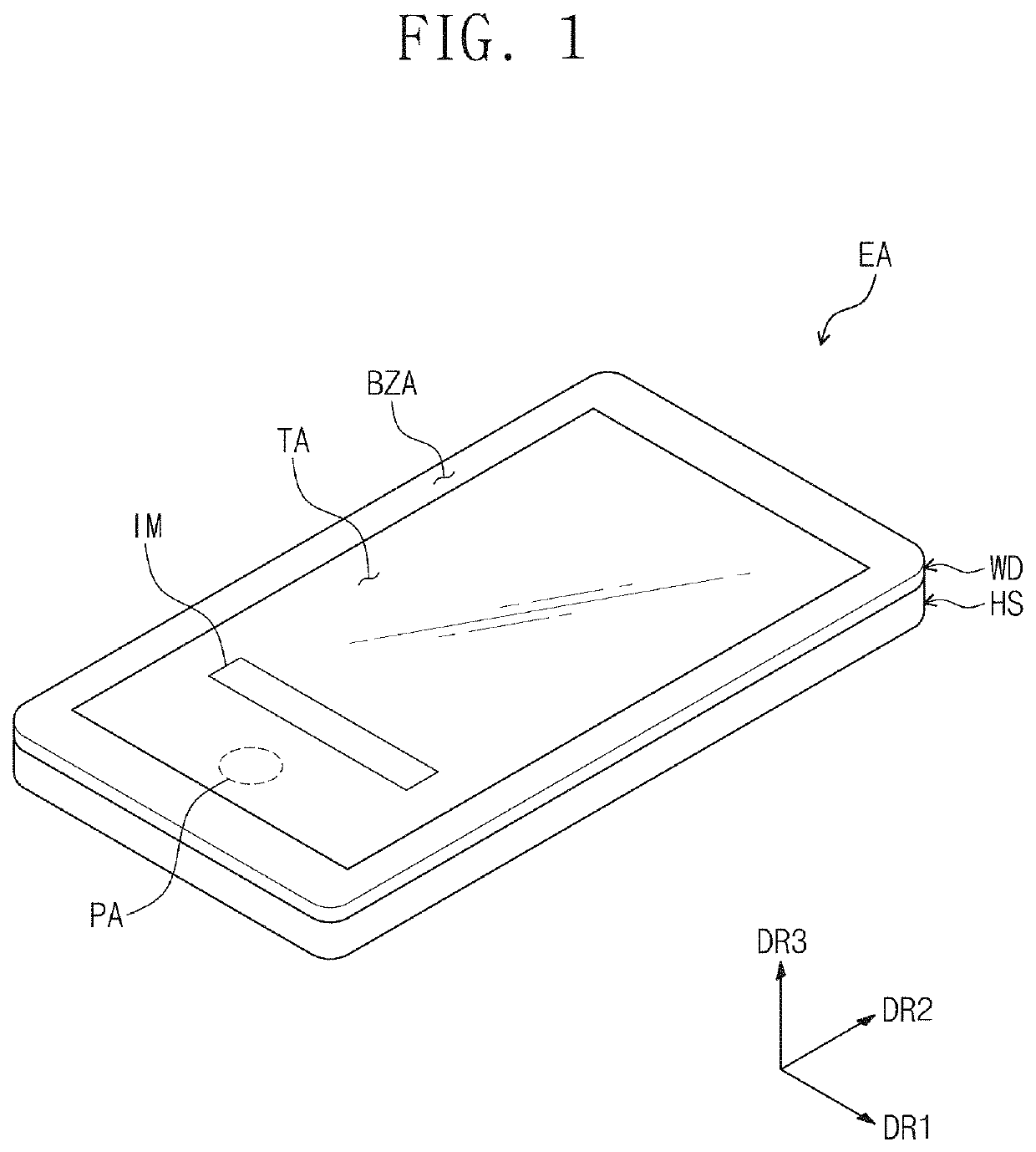
[0040]The invention now will be described more fully hereinafter with reference to the accompanying drawings, in which various embodiments are shown. The invention may, however, be embodied in many different forms, and should not be construed as limited to the embodiments set forth herein. Rather, these embodiments are provided so that this disclosure will be thorough and complete, and will fully convey the scopes of the invention to those skilled in the art. Like reference numerals refer to like elements throughout.

[0041]In this specification, it will also be understood that when one component (or region, layer, portion) is referred to as being ‘on’, ‘connected to’, or ‘coupled to’ another component, it can be directly disposed / connected / coupled on / to the one component, or an intervening third component may also be present.

[0042]The terminology used herein is for the purpose of describing particular embodiments only and is not intended to be limiting. As used herein, the singular f...


PUM

PropertyMeasurementUnit
thicknessaaaaaaaaaa
areaaaaaaaaaaa
area TTaaaaaaaaaa

Abstract

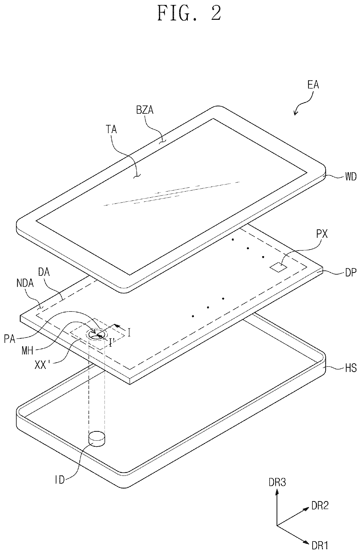
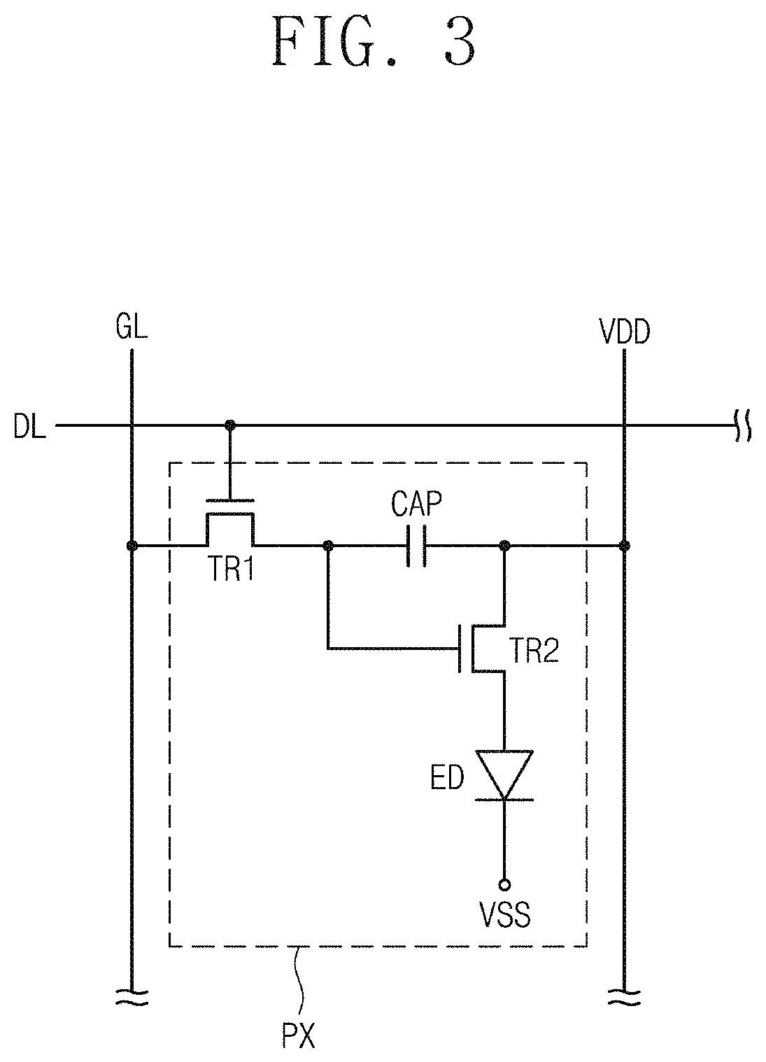
A display panel includes a base substrate including a display area surrounding a hole area, a circuit layer including insulation layers, where an opening is defined through each insulation layer to overlap the hole area, an element layer including an organic light emitting element connected to a transistor, an encapsulation layer disposed on the element layer and including first and second encapsulation inorganic layers and an organic layer, a cover inorganic layer overlapping the hole area and disposed between the first encapsulation inorganic layer and the insulation layers. A module hole is defined through the display panel, and a first groove is defined by portions of the cover inorganic layer and the first and second encapsulation inorganic layers which cover inner surface of the opening and the recess part. The cover inorganic layer contacts the inner surfaces of the opening and the recess part.

Description

[0001]This application claims priority to Korean Patent Application No. 10-2018-0114930, filed on Sep. 27, 2018, and all the benefits accruing therefrom under 35 U.S.C. § 119, the content of which in its entirety is herein incorporated by reference.BACKGROUND1. Field[0002]The disclosure herein relates a display panel and an electronic device including the display panel, and more particularly, to a display panel having improved reliability and an electronic device including the display panel.2. Description of the Related Art[0003]A display panel may be activated according to an electrical signal to display an image. Such a display panel may be an organic light emitting display panel including an organic light emitting element that has low power consumption, high luminance, and a high response speed.SUMMARY[0004]An organic light emitting display panel includes an organic light emitting element. The organic light emitting element may be vulnerable to moisture or oxygen and thus easily ...

Claims


Application Information

Patent Timeline
Patent Type & Authority Patents(United States)
IPC IPC(8): H01L51/00H01L27/00H01L51/52H01L27/32
CPCH01L51/0097H01L27/3244H01L51/5253H01L2227/323H10K50/84Y02E10/549H10K59/65H10K59/124H10K59/121H10K50/80H10K50/844H10K59/00H10K71/00H10K59/12H10K77/111H10K59/1201
Inventor KIM, NAMJIN
Owner SAMSUNG DISPLAY CO LTD
Learn More