
Micro light emitting diode display panel

a light-emitting diode and display panel technology, applied in the field of display, can solve the problems of thinness and shape, color filter substrate consumes at least 60% of light energy, and the liquid crystal display device of the prior art is hardly thinner and flexible, so as to achieve a large amount of light energy, shape, and reduce the effect of thickness

Active Publication Date: 2020-04-28
WUHAN CHINA STAR OPTOELECTRONICS TECH CO LTD
View PDF3 Cites 0 Cited by
  • Summary
  • Abstract
  • Description
  • Claims
  • Application Information

AI Technical Summary

Benefits of technology

The solution allows for a thinner, more flexible display panel that reduces power consumption by eliminating the need for a backlight and color filter, while achieving desired brightness and color through efficient light management.

Problems solved by technology

These stacked structures limit the thickness and shape of liquid crystal display devices of the prior art, resulting in that the liquid crystal display devices of the prior art are hardly thinner and more flexible.
In addition, the color filter substrate consumes at least 60% of the light energy.
Thus, it only can rely on increasing the backlight brightness of the liquid crystal display device to satisfy the brightness requirement of the actual device, which undoubtedly increases the power consumption of the liquid crystal display device.

Method used


Image

  • Micro light emitting diode display panel
  • Micro light emitting diode display panel
  • Micro light emitting diode display panel

Examples


Embodiment Construction

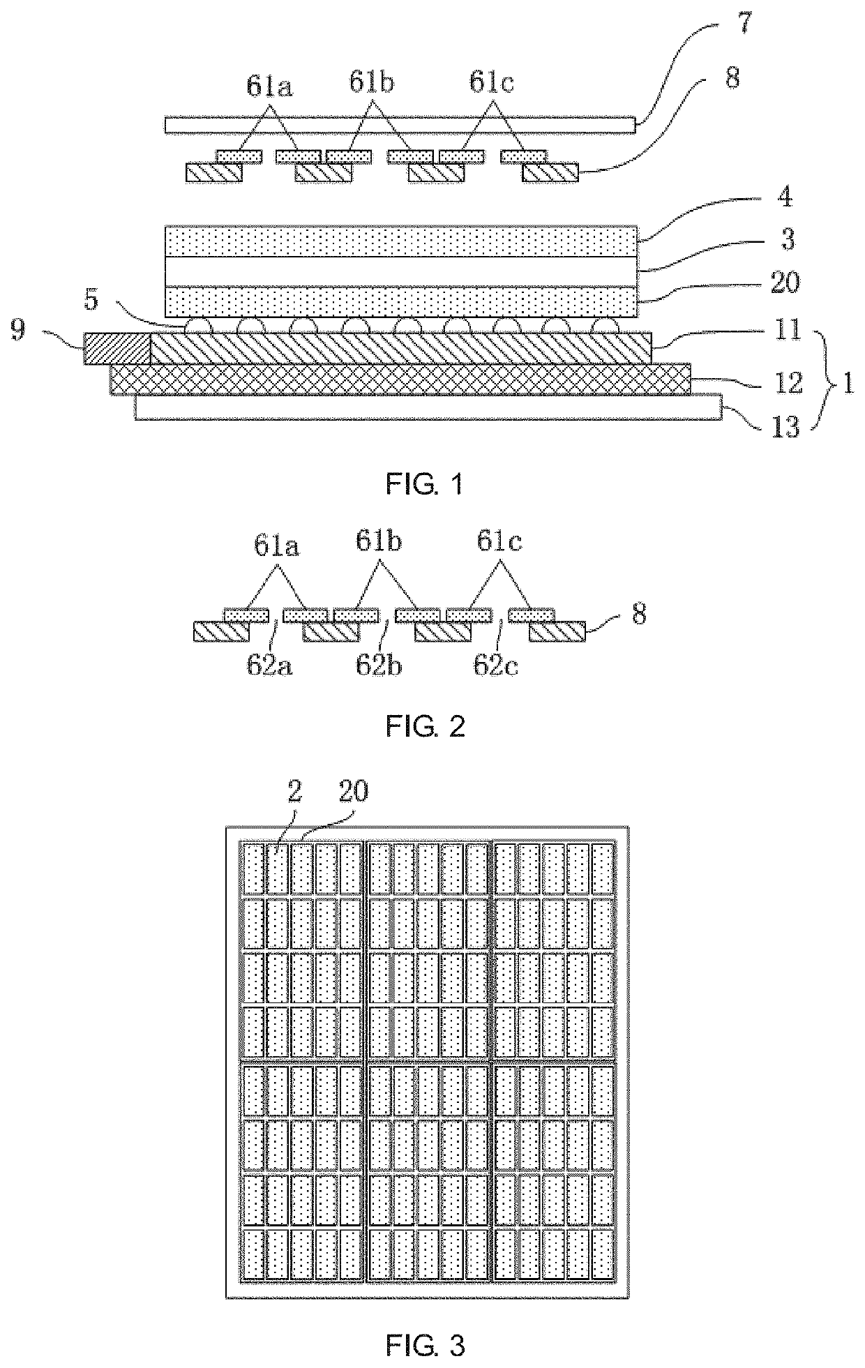
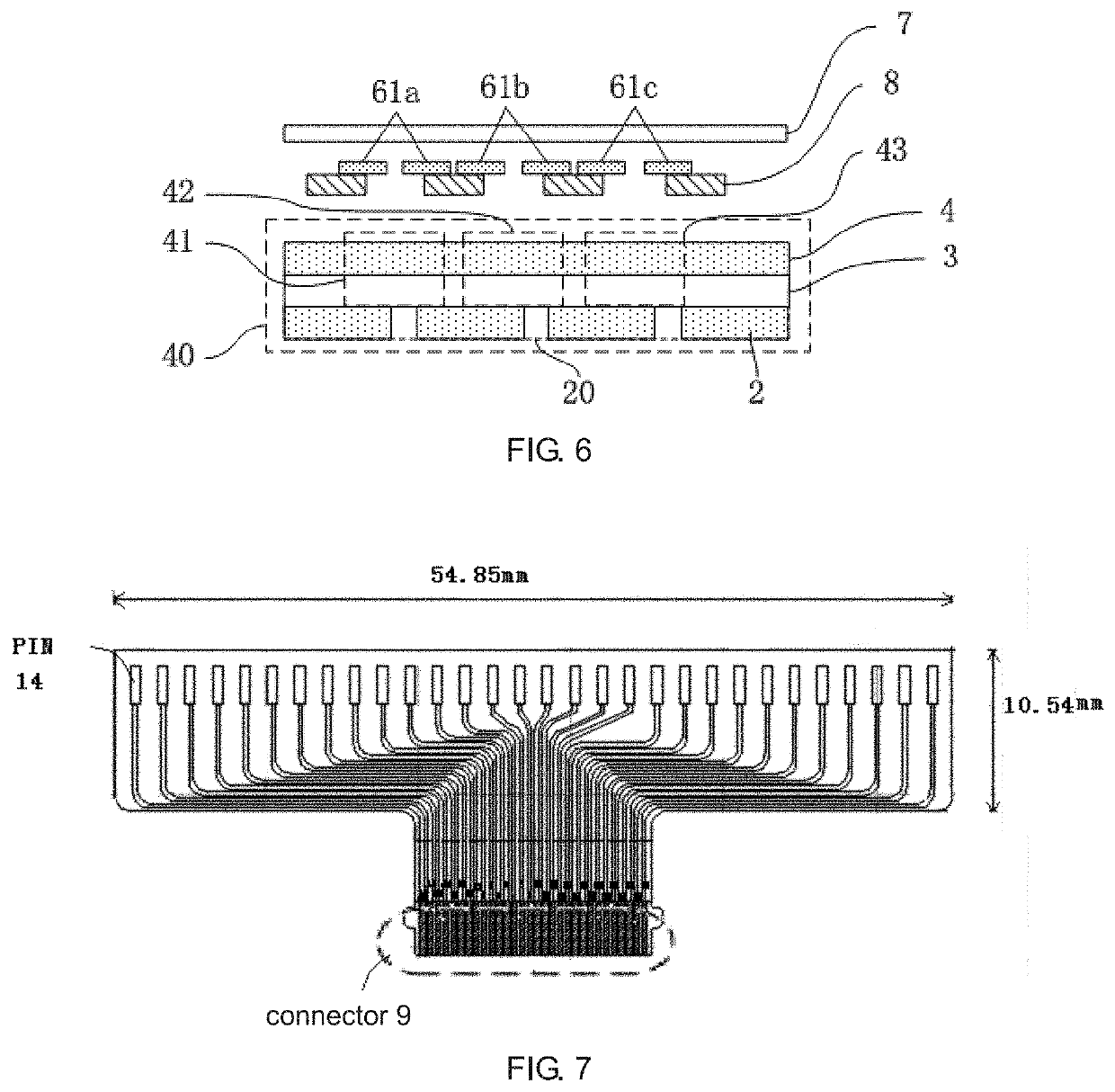
[0040]The present invention provides a micro light emitting diode display panel as shown in FIG. 2. The display panel comprises a flexible substrate 1, a plurality of light emitting diodes 2 aligned in an array, a diffraction grating 3 and a light scattering film 4 arranged on the plurality of light emitting diodes 2 and a plurality of light valves arranged above the light scattering film 4. The labels 61a, 61b and 61c shown in FIG. 1 are light valves. As shown in FIG. 2, the corresponding openings of the light valves 61a, 61b and 61c are 62a, 62b and 62c, respectively.

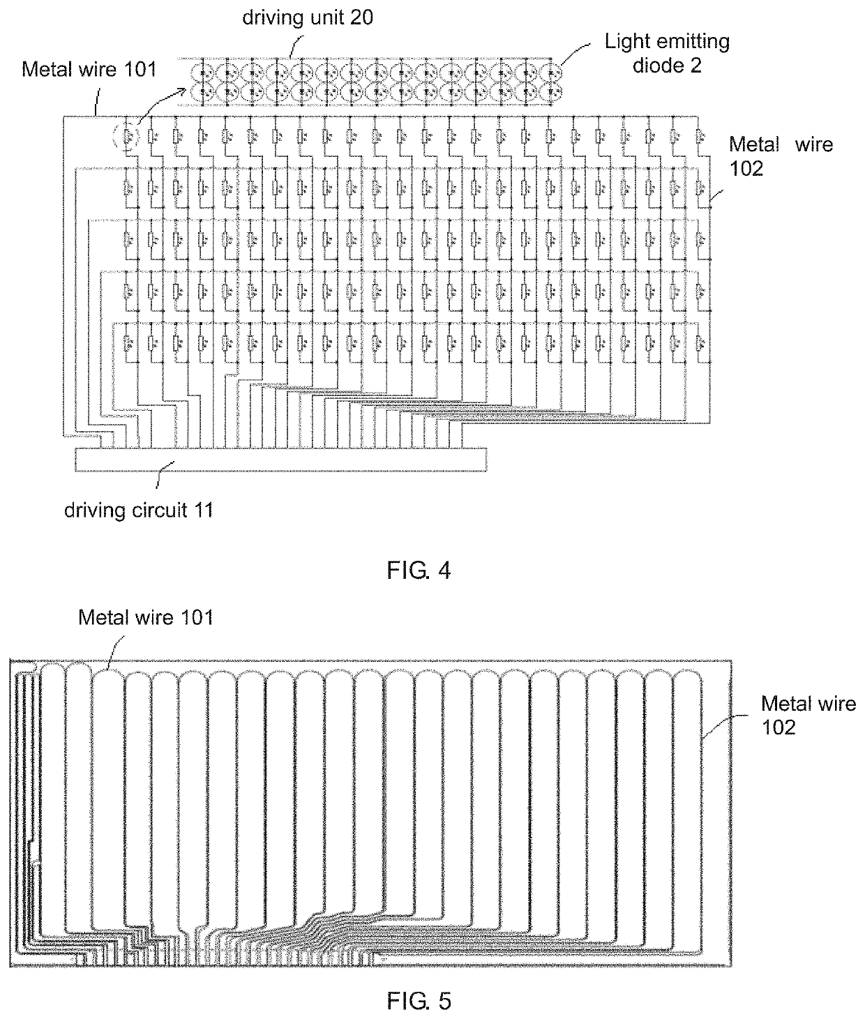
[0041]The flexible substrate 1 comprises a driving circuit 11, the plurality of light emitting diodes 2 are fixed on the flexible substrate 1 by flip chip; the driving circuit 11 is connected to the plurality of light emitting diodes 2 to respectively drive the plurality of light emitting diodes 2 to emit white light.

[0042]The diffraction grating 3 splits the white light emitted by the light emitting diodes 2 to form ...


PUM

PropertyMeasurementUnit
thicknessaaaaaaaaaa
widthaaaaaaaaaa
flexibleaaaaaaaaaa

Abstract

Provided is a micro light emitting diode display panel, comprising a flexible substrate, light emitting diodes aligned in an array, a diffraction grating and a light scattering film arranged on the light emitting diodes and light valves arranged above the light scattering film; wherein the flexible substrate comprises a driving circuit, the light emitting diodes are fixed on the flexible substrate; the driving circuit is connected to the light emitting diodes to respectively drive the light emitting diodes to emit white light; the diffraction grating splits the white light emitted by the light emitting diodes to form exiting lights with various wavelengths; the light scattering film gathers an exiting light of a same wavelength in the exiting lights and disperses the exiting lights of different wavelengths to form a primary color light of at least one color; the light valves adjusts an intensity of the primary color light.

Description

CROSS-REFERENCE TO RELATED APPLICATION[0001]This application is a continuing application of PCT Patent Application No. PCT / CN2018 / 079005 entitled “Micro light emitting diode display panel”, filed on Mar. 14, 2018, which claims priority to Chinese Patent Application No. 201810135165.8, filed on Feb. 9, 2018, both of which are hereby incorporated in its entireties by reference.FIELD OF THE INVENTION[0002]The present invention relates to a display field, and more particularly to a micro light emitting diode display panel.BACKGROUND OF THE INVENTION[0003]At present, being light, thin and convenient, energy-saving, exquisite pictures, reduced costs, and diversified functions are always the development goals of display devices. Meanwhile, as dedicating to provide various types of electronic devices, research and development have been conducted to provide various forms of display devices included in the electronic devices. The existing liquid crystal display device of the prior art include...

Claims


Application Information

Patent Timeline
Patent Type & Authority Patents(United States)
IPC IPC(8): G02B5/02H01L25/16G09G3/32G02B27/42G02B5/18H05K1/18H05K1/14
CPCG02B5/1814G09G3/32G02B27/425G02B5/0278H01L25/167H05K2201/041G09G2380/02H05K1/189H05K1/147H05K2201/10128G09G2330/021H05K2201/10106H05K2201/10166H05K1/144G09G2320/0626
Inventor CHENG, YAN
Owner WUHAN CHINA STAR OPTOELECTRONICS TECH CO LTD
Learn More