Semiconductor manufacturing apparatus and method of manufacturing semiconductor device using the same

a manufacturing apparatus and semiconductor technology, applied in the direction of lapping machines, instruments, image enhancement, etc., can solve the problems of increasing the demand for thin wafers, increasing the possibility of physical defects on the wafer, and affecting etc., to achieve the effect of weakening the adhesive strength of ultraviolet sensitive layers

Active Publication Date: 2020-04-14
SAMSUNG ELECTRONICS CO LTD
View PDF22 Cites 0 Cited by
  • Summary
  • Abstract
  • Description
  • Claims
  • Application Information

AI Technical Summary

Problems solved by technology

Accordingly, a defect such as a crack may occur in the wafer.
In recent years, there has been an increase in the demand for thin wafers, and according to the development trend of products, both the demand for thin wafers and the possibility of occurrence of physical defects on the wafer are also increasing.

Method used


Image

  • Semiconductor manufacturing apparatus and method of manufacturing semiconductor device using the same
  • Semiconductor manufacturing apparatus and method of manufacturing semiconductor device using the same
  • Semiconductor manufacturing apparatus and method of manufacturing semiconductor device using the same

Examples


Embodiment Construction

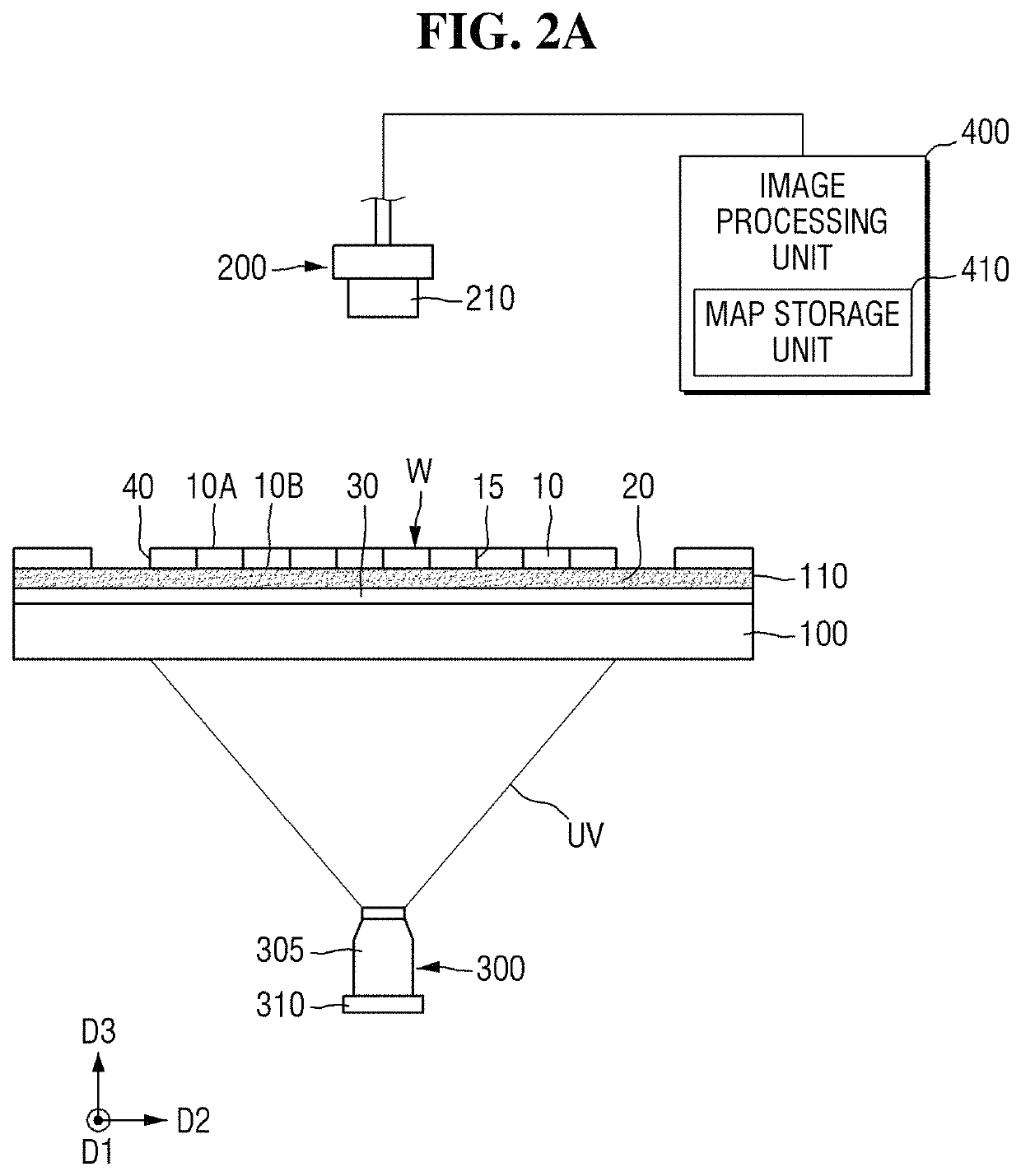
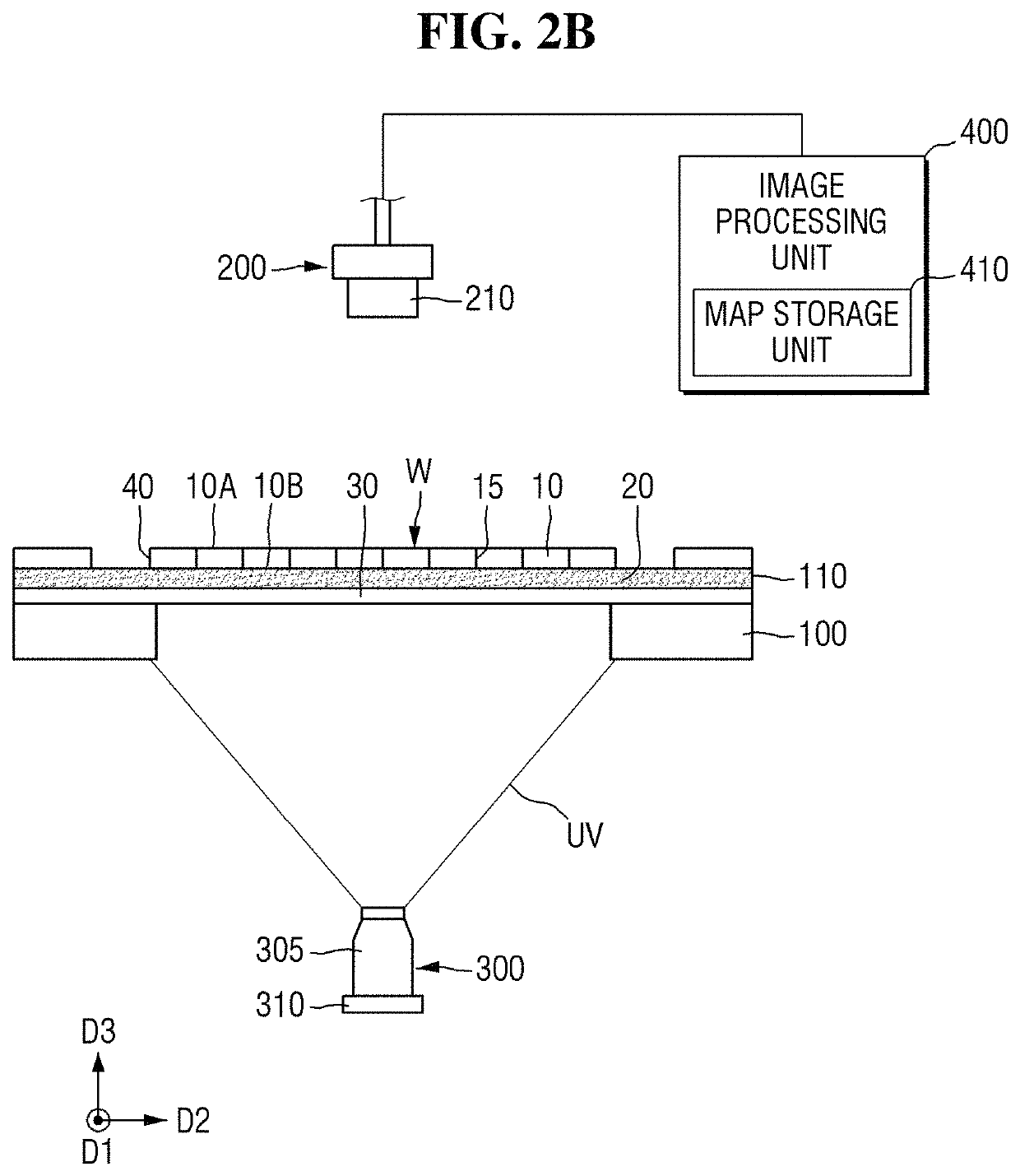
[0025]Hereinafter, a semiconductor manufacturing apparatus and a semiconductor manufacturing method using the same according to some embodiments of the present inventive concept will be described with reference to FIGS. 1 to 13.

[0026]FIG. 1 is a perspective view of a semiconductor manufacturing apparatus according to an exemplary embodiment of the present inventive concept. FIG. 2 is a conceptual diagram explaining the semiconductor manufacturing apparatus of FIG. 1.

[0027]Referring to FIGS. 1 and 2A-2B, a semiconductor manufacturing apparatus according to an exemplary embodiment of the present inventive concept may include a loading unit 100, an optical device such as a camera 200, an ultraviolet light source 300, an image processing unit 400 and the like.

[0028]The loading unit 100 may load the wafer W thereon. The loading unit 100 may include a transparent material that transmits ultraviolet light (UV) emitted from the ultraviolet light source 300. In the exemplary embodiment, the ...


PUM

PropertyMeasurementUnit
wavelength rangeaaaaaaaaaa
wavelength bandaaaaaaaaaa
exposure timeaaaaaaaaaa

Abstract

A semiconductor manufacturing apparatus and a method of manufacturing semiconductor device are provided. The semiconductor manufacturing apparatus includes a loading unit configured to load a wafer having a first surface to which a die attach film is attached through an ultraviolet sensitive layer, an ultraviolet light source configured to irradiate ultraviolet light onto the first surface of the wafer attached to the die attach film to weaken adhesive strength of the ultraviolet sensitive layer, and a camera configured to generate a wafer image by capturing ultraviolet light transmitted through a second surface of the wafer opposite to the first surface of the wafer.

Description

CROSS-REFERENCE TO RELATED APPLICATION[0001]This application claims priority from Korean Patent Application No. 10-2017-0106810 filed on Aug. 23, 2017 in the Korean Intellectual Property Office, and all the benefits accruing therefrom under 35 U.S.C. 119, the contents of which are incorporated herein by reference in its entirety.BACKGROUND1. Technical Field[0002]The present disclosure relates to a semiconductor manufacturing apparatus and a method of manufacturing a semiconductor device using the same.2. Description of the Related Art[0003]Various physical and chemical loads are applied to a wafer in a semiconductor manufacturing process. Particularly in a semiconductor packaging process, a back lap (B / L) process, a grind after laser (GAL) process or the like causes a physical impact on a wafer to process the surface of a semiconductor device. Accordingly, a defect such as a crack may occur in the wafer.[0004]In recent years, there has been an increase in the demand for thin wafers,...

Claims


Application Information

Patent Timeline
Patent Type & Authority Patents(United States)
IPC IPC(8): H01L21/268H01L21/66H01L23/544H01L21/67H01L21/683H01L21/78H01L21/304G06T7/00B24B37/005B23K26/364B23K101/40
CPCH01L23/544H01L21/78H01L21/6836H01L21/6835G06T7/0004H01L21/268H01L21/67115H01L22/12H01L21/304H01L21/67288G06T2207/10144H01L2223/5446B24B37/0053G06T2207/30148H01L21/67092B23K2101/40B23K26/364H01L2221/68327G06T2207/20221H01L21/67132B23K26/359B23K26/53B23K26/402B23K26/0006B23K2103/56H01L22/24H01L22/30H01L21/76
Inventor HA, KYUNG HO
Owner SAMSUNG ELECTRONICS CO LTD
Why Eureka
Try Eureka