Conductive film for touch panel, touch panel, and touch panel-equipped display device
a technology of touch panel and conductive film, which is applied in the direction of instruments, computing, electric digital data processing, etc., can solve the problems of significant moire and noise, productivity and cost, etc., and achieve the effect of reducing moire and nois
- Summary
- Abstract
- Description
- Claims
- Application Information
AI Technical Summary
Benefits of technology
Problems solved by technology
Method used
Image
Examples
example 1
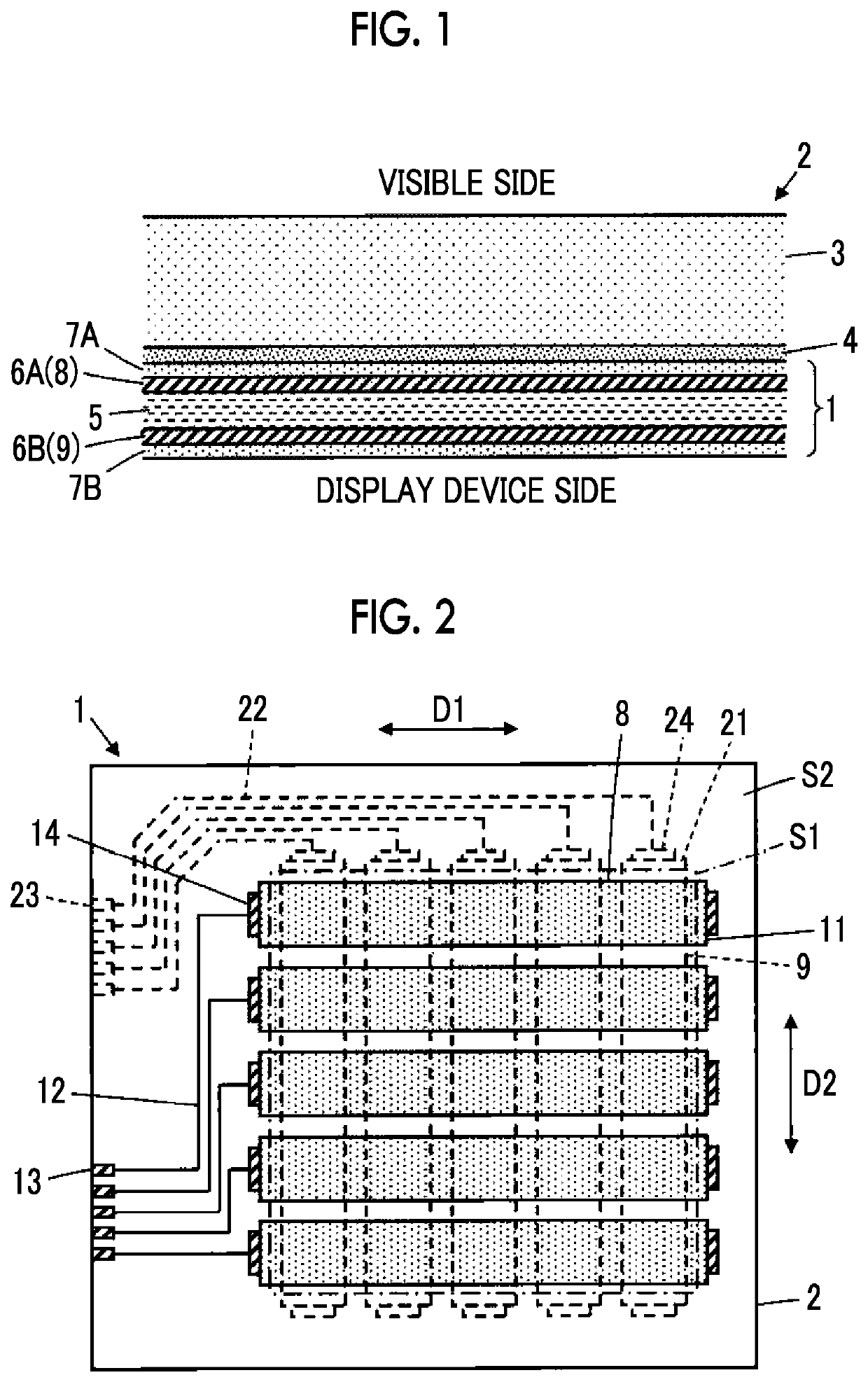
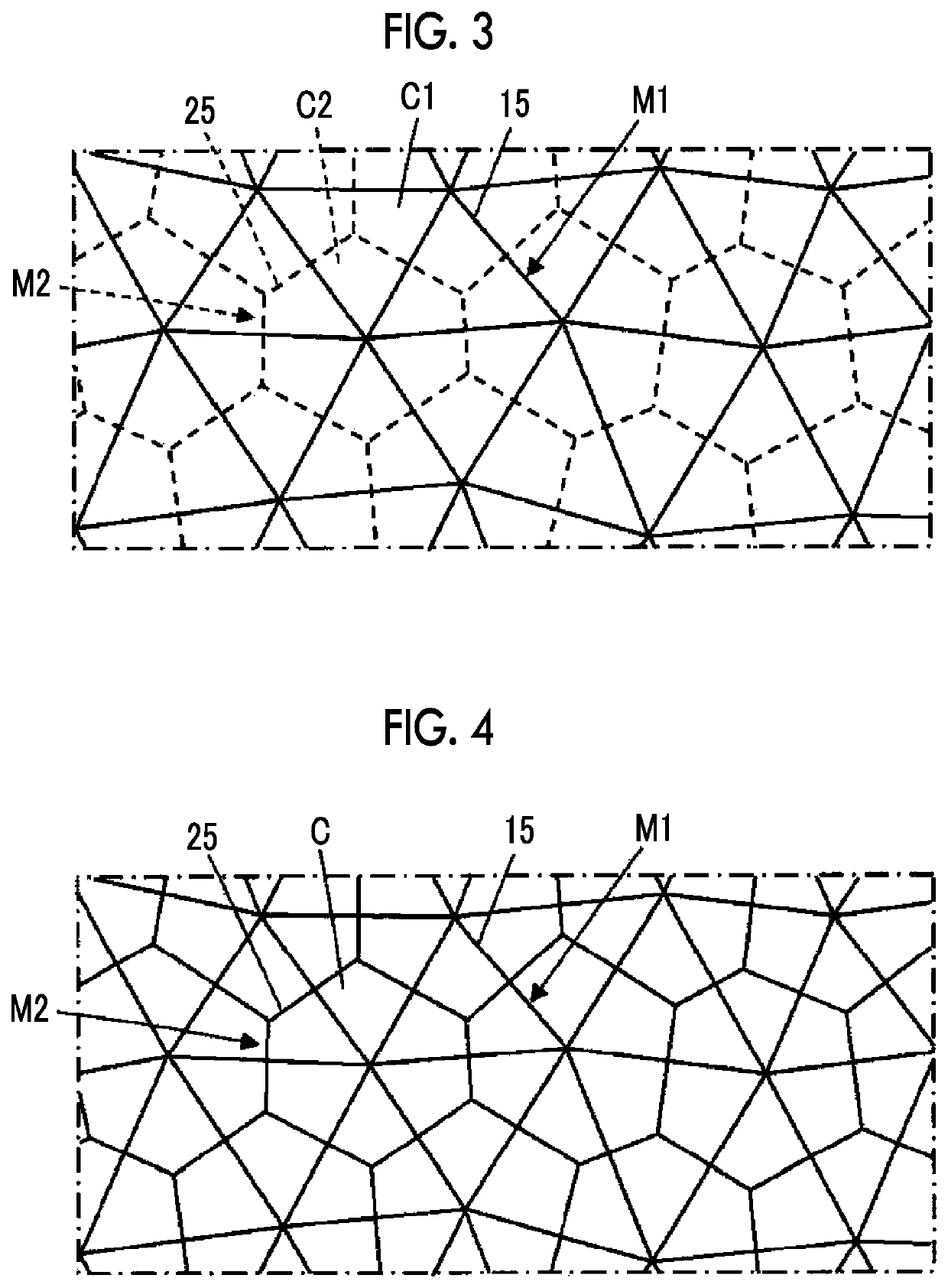
[0178]The first mesh pattern M1 and the second mesh pattern M2 were designed using the above-described design method such that the average line width of the first thin metal wire 15 and the second thin metal wire 25 was 2.0 μm, the initial inter-apex distance L0 when the regular triangles T were disposed was 500 μm, and the movement tolerance R of the apex was 100 μm. That is, a plurality of triangles having randomness were formed based on the movement tolerance R of the apex, and circumcenters of the triangles were connected to each other. As a result, the second cells C2 of the second mesh pattern M2 were formed, and the first cells C1 of the first mesh pattern M1 were formed using the triangles.
[0179]In order to design a mesh pattern, a unit mesh pattern having a size of 5.0 mm×5.0 mm, which was the minimum electrode pitch, was formed, and the entire mesh pattern in the active area was formed by repeatedly using the unit mesh pattern.
[0180]The first conductive layer 8 in which th...
example 42
[0267]A mesh pattern was formed by combining the 5.0 mm×5.0 mm unit mesh pattern used in Example 1 and the 5.0 mm×5.0 mm unit mesh pattern used in Example 5. Under the same conditions as in Example 1 except for the mesh pattern, the preparation, the evaluation, the evaluation of opening ratio uniformity were performed.
(Result of Evaluation of Opening Ratio Uniformity)
[0268]In the conductive films for a touch panel according to Examples 1 to 41, all the results were 0.4% or lower. However, the result of conductive film for a touch panel according to Example 42 was 1.1%.
[0269]In the evaluations of moire, noise, and mesh appearance, the results of Example 42 were A. However, in a case where a white solid image was displayed using the display devices, unevenness in the luminance of the display devices were recognized as compared to the conductive films for a touch panel according to Examples 1 to 41.
[0270]In Examples, both the first mesh pattern M1 and the second mesh pattern M2 were ra...
PUM
| Property | Measurement | Unit |
|---|---|---|
| width | aaaaa | aaaaa |
| visible light reflectivity | aaaaa | aaaaa |
| width | aaaaa | aaaaa |
Abstract
Description
Claims
Application Information
 - R&D
- Intellectual Property
- Life Sciences
- Materials
- Tech Scout
- Unparalleled Data Quality
- Higher Quality Content
- 60% Fewer Hallucinations
Browse by: Latest US Patents, China's latest patents, Technical Efficacy Thesaurus, Application Domain, Technology Topic, Popular Technical Reports.
© 2025 PatSnap. All rights reserved.Legal|Privacy policy|Modern Slavery Act Transparency Statement|Sitemap|About US| Contact US: help@patsnap.com


