
Conductive member, touch panel, and display device

a touch panel and display device technology, applied in semiconductor devices, instruments, computing, etc., can solve the problem of remarkable visual recognition of moire, and achieve the effect of reducing moir

Active Publication Date: 2021-07-27
FUJIFILM CORP
View PDF31 Cites 0 Cited by
  • Summary
  • Abstract
  • Description
  • Claims
  • Application Information

AI Technical Summary

Benefits of technology

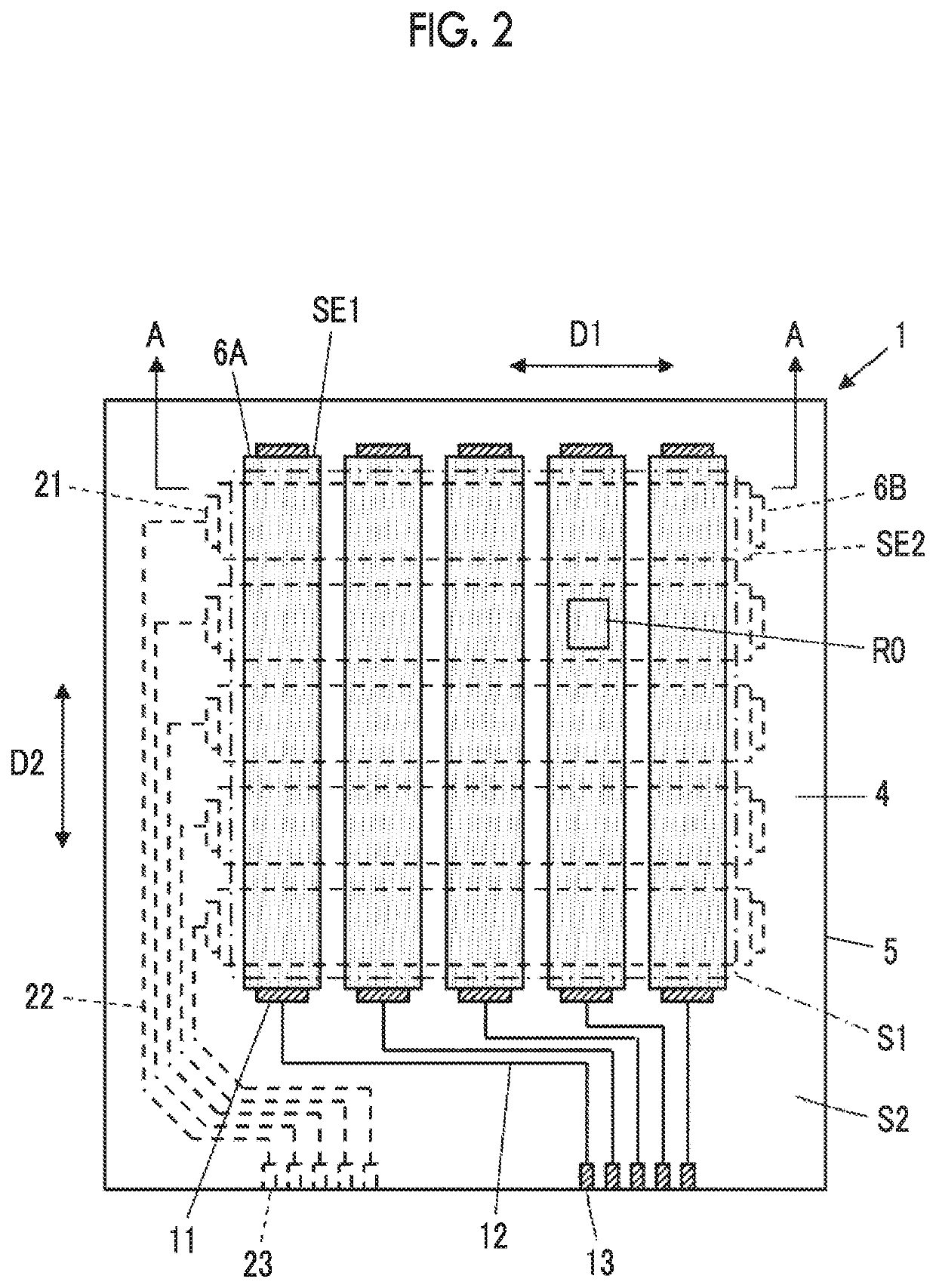
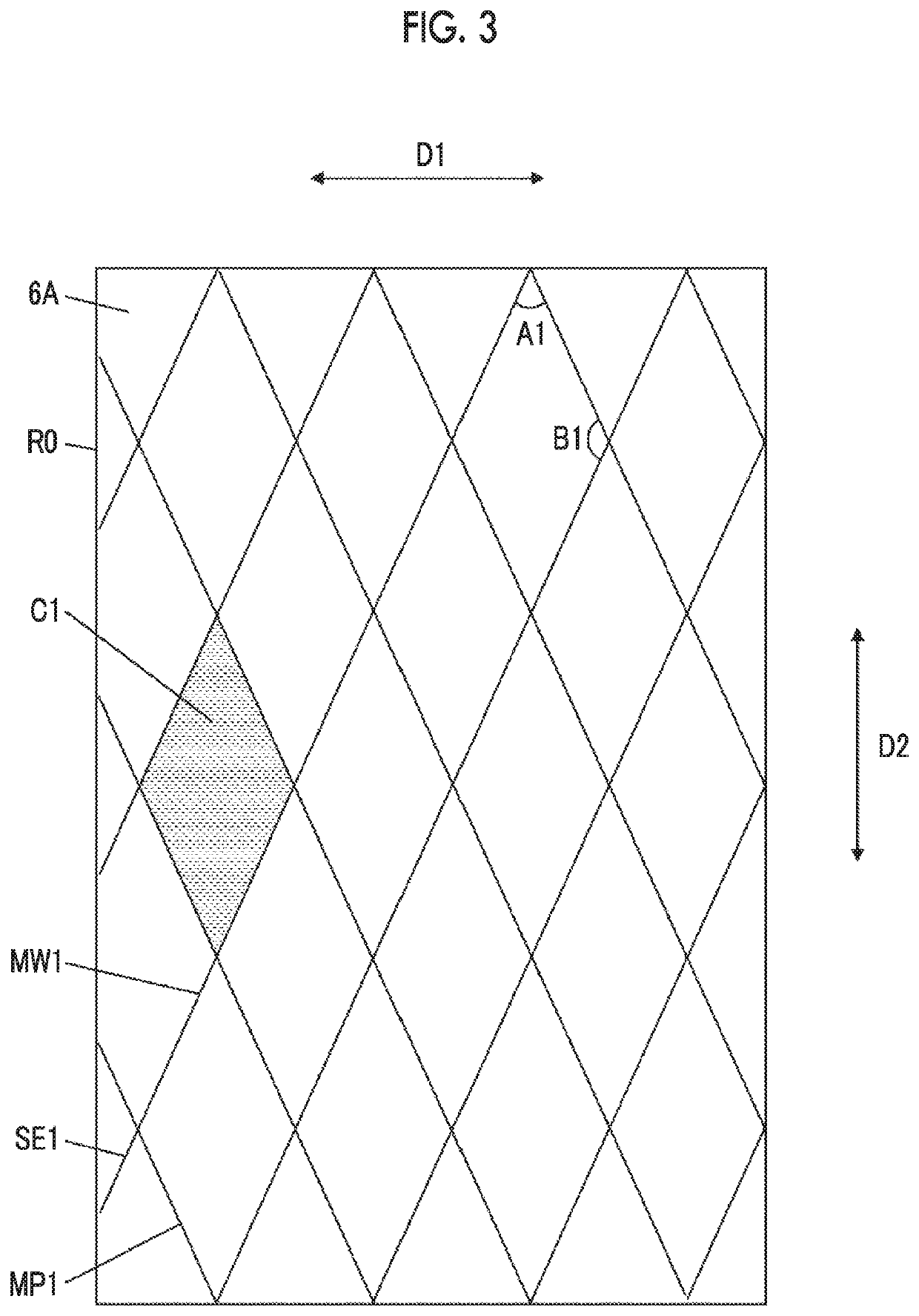
[0017]According to the present invention, since a mesh pattern is formed by the plurality of thin metal wires in a case of being viewed from a direction perpendicular to the transparent insulating substrate, the mesh pattern is constituted by the plurality of quadrangular mesh cells having two acute angles of less than 90 degrees and two obtuse angles of more than 90 degrees, and the degree of the acute angles is 44 degrees or more and 54 degrees or less, it is possible to reduce moire in a display panel in which a plurality of pixels are arrayed in a mosaic array and a delta array.

Problems solved by technology

In a case where the conductive member disclosed in JP2012-164648A is used for such a display panel, there is a problem that moire is remarkably visually recognized.

Method used


Image

  • Conductive member, touch panel, and display device
  • Conductive member, touch panel, and display device
  • Conductive member, touch panel, and display device

Examples


embodiments

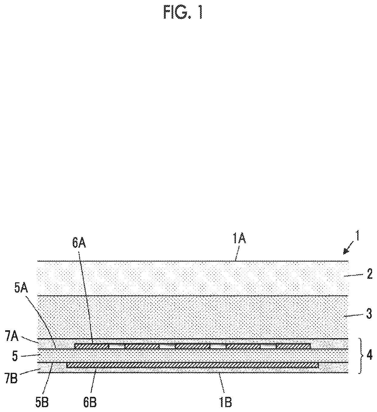
[0029]FIG. 1 shows a configuration of a touch panel 1 according to an embodiment of the present invention. The touch panel 1 has a front surface 1A and a back surface 1B, and a display panel described later is arranged on the back surface 1B side to constitute a display device. The front surface 1A of the touch panel 1 is a touch surface for detecting a touch operation, and is a viewing side where an operator of the touch panel 1 observes an image displayed on the display device through the touch panel 1. The touch panel 1 has a transparent insulating cover panel 2 arranged on the front surface 1A side, and a conductive member 4 is bonded onto a surface of the cover panel 2 opposite to the front surface 1A via a transparent adhesive layer 3.

[0030]The conductive member 4 has a transparent insulating substrate 5, and the transparent insulating substrate 5 has a first surface 5A facing the front surface 1A side of the touch panel 1 and a second surface 5B facing a side opposite to the ...

example 1

[0118]Example 1 was a touch panel having the same configuration as the touch panel 1 according to the embodiment of the present invention shown in FIGS. 1 to 5, and the degree of the acute angles A3 of the rhombic third mesh cell C3 was set to 44 degrees.

example 2

[0119]Example 2 was the same as Example 1 except that the degree of the acute angles A3 of the rhombic third mesh cell C3 was set to 46 degrees.


PUM

PropertyMeasurementUnit
obtuse anglesaaaaaaaaaa
acute anglesaaaaaaaaaa

Abstract

A conductive member is arranged on a display panel in which a plurality of pixels are arrayed in a mosaic array or a delta array, and includes a transparent insulating substrate and at least one conductive layer which has a plurality of thin metal wires and is arranged on the transparent insulating substrate, in a case of being viewed from a direction perpendicular to the transparent insulating substrate, a mesh pattern is formed by the plurality of thin metal wires, the mesh pattern is constituted by a plurality of quadrangular mesh cells having two acute angles of less than 90 degrees and two obtuse angles of more than 90 degrees, and a degree of the acute angles is 44 degrees or more and 54 degrees or less.

Description

CROSS-REFERENCE TO RELATED APPLICATIONS[0001]This application is a Continuation of PCT International Application No. PCT / JP2018 / 040106 filed on Oct. 29, 2018, which was published under PCT Article 21(2) in Japanese, and which claims priority under 35 U.S.C. § 119(a) to Japanese Patent Application No. 2017-238573 filed on Dec. 13, 2017. The above applications are hereby expressly incorporated by reference, in their entirety, into the present application.BACKGROUND OF THE INVENTION1. Field of the Invention[0002]The present invention relates to a conductive member arranged on a display panel in which a plurality of pixels are arrayed in a mosaic array or a delta array, a touch panel including the conductive member, and a display device.2. Description of the Related Art[0003]In recent years, touch panels which are used by being combined with a display device such as a liquid crystal display device in various kinds of electronic devices including portable information devices such as tabl...

Claims


Application Information

Patent Timeline
Patent Type & Authority Patents(United States)
IPC IPC(8): G06F3/044G06F3/047H01L27/32
CPCG06F3/0446G06F3/047H01L27/3218G06F2203/04112G06F3/0445H10K59/352H10K59/353H10K59/40G06F3/044
Inventor HARA, DAISUKEKATSUYAMA, KIMITONAKAYAMA, MASAYA
Owner FUJIFILM CORP
Learn More