Semiconductor device and method for fabricating the same

a technology of semiconductor devices and fuse structures, applied in the direction of semiconductor devices, electrical equipment, transistors, etc., can solve the problems that current dram units with buried gate structures still pose numerous problems

Active Publication Date: 2019-11-12
UNITED MICROELECTRONICS CORP +1
View PDF3 Cites 7 Cited by
  • Summary
  • Abstract
  • Description
  • Claims
  • Application Information

AI Technical Summary

Benefits of technology

The present invention provides a method and a semiconductor device that allows for improved fabrication of a bit line structure. The method involves forming a spacer adjacent to the bit line structure and an interlayer dielectric layer adjacent to the spacer. The interlayer dielectric layer is then removed to expose a sidewall of the bit line structure. A storage node contact isolation structure is then formed, which directly contacts the bit line structure and the spacer. The semiconductor device includes a bit line structure, a spacer, and a storage node contact isolation structure that all extend along a specific direction on the substrate. The technical effect of this invention is to facilitate the fabrication of semiconductor devices that have reliable and efficient bit line structures.

Problems solved by technology

Nevertheless, current DRAM units with buried gate structures still pose numerous problems due to limited fabrication capability.

Method used


Image

  • Semiconductor device and method for fabricating the same
  • Semiconductor device and method for fabricating the same
  • Semiconductor device and method for fabricating the same

Examples


Embodiment Construction

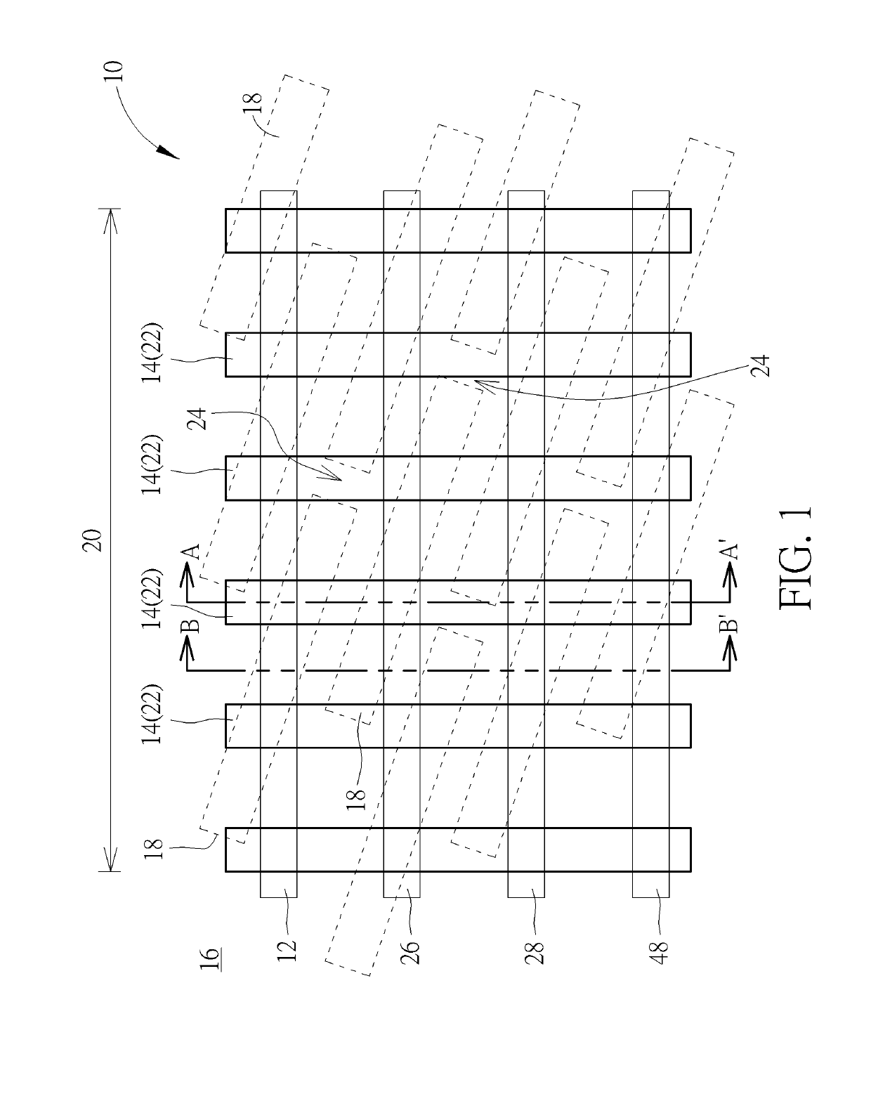
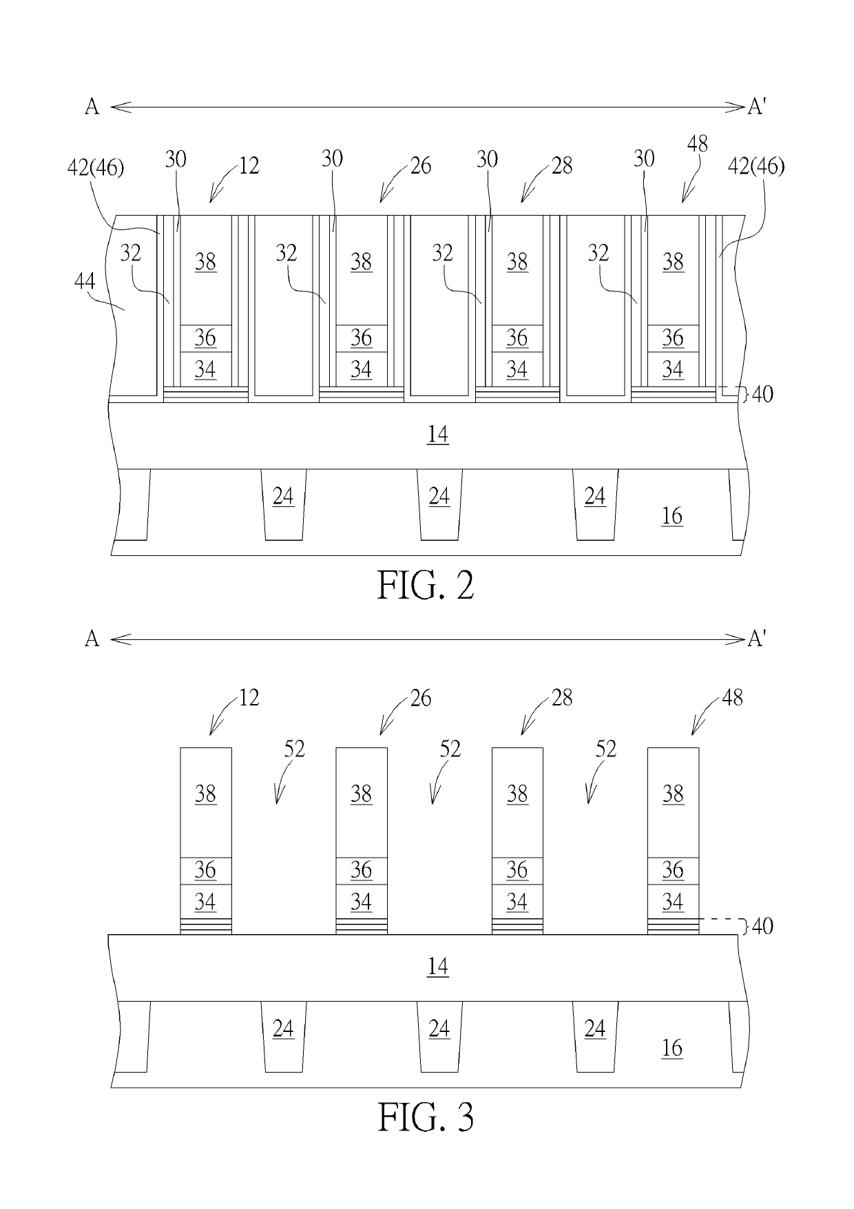
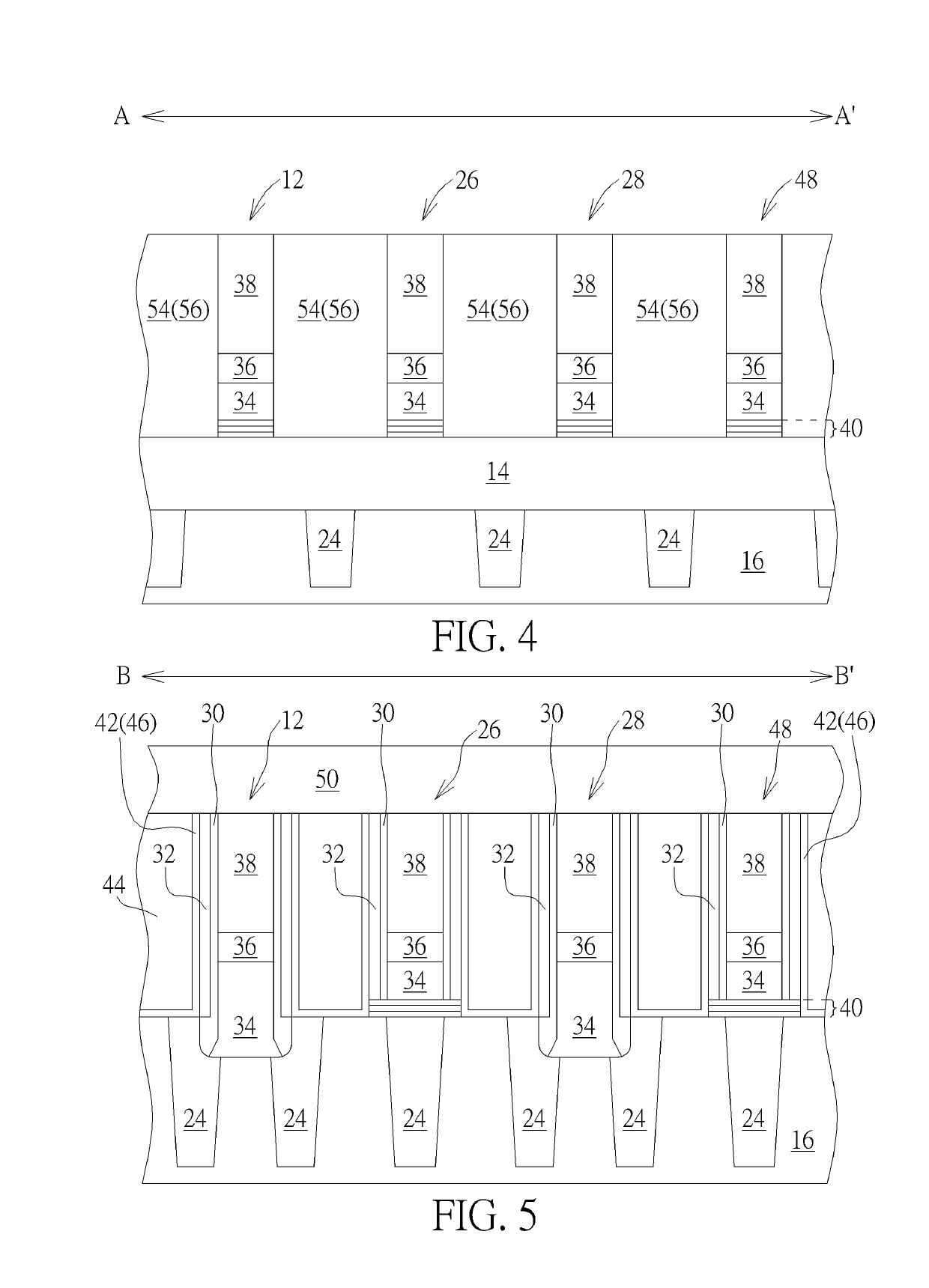
[0011]Referring to FIGS. 1-8, FIGS. 1-8 illustrate a method for fabricating a DRAM device according to an embodiment of the present invention, in which FIG. 1 illustrates a top-view diagram of a DRAM device, FIGS. 2-4 illustrate cross-section views of a method for fabricating a DRAM device along the sectional line AA′ of FIG. 1, FIGS. 5-7 illustrate cross-section views of a method for fabricating a DRAM device along the sectional line BB′ of FIG. 1, and FIG. 8 illustrates an enlarged top view of two adjacent bit line structures shown in FIG. 1.

[0012]Preferably, the present embodiment pertains to fabricate a memory device, and more particularly a DRAM device 10, in which the DRAM device 10 includes at least a transistor device (not shown) and at least a capacitor structure (not shown) that will be serving as a smallest constituent unit within the DRAM array and also used to receive electrical signals from bit lines 12, 26, 28, 48 and word lines 14.

[0013]As shown in FIG. 1, the DRAM d...


PUM


Abstract

A method for fabricating semiconductor device includes the steps of: forming a first bit line structure on a substrate; forming a first spacer adjacent to the first bit line structure; forming an interlayer dielectric (ILD) layer adjacent to the first spacer; removing part of the ILD layer and part of the first spacer to expose a sidewall of the first bit line structure; and forming a first storage node contact isolation structure adjacent to the first bit line structure, wherein the first storage node contact isolation structure contacts the first bit line structure and the first spacer directly.

Description

BACKGROUND OF THE INVENTION1. Field of the Invention[0001]The invention relates to a method for fabricating semiconductor device, and more particularly, to a method of fabricating fuse structure of a dynamic random access memory (DRAM) device.2. Description of the Prior Art[0002]As electronic products develop toward the direction of miniaturization, the design of dynamic random access memory (DRAM) units also moves toward the direction of higher integration and higher density. Since the nature of a DRAM unit with buried gate structures has the advantage of possessing longer carrier channel length within a semiconductor substrate thereby reducing capacitor leakage, it has been gradually used to replace conventional DRAM unit with planar gate structures.[0003]Typically, a DRAM unit with buried gate structure includes a transistor device and a charge storage element to receive electrical signals from bit lines and word lines. Nevertheless, current DRAM units with buried gate structures...

Claims


Application Information

Patent Timeline
IPC IPC(8): H01L27/108H01L21/762
CPCH01L27/10891H01L21/762H01L27/10888H01L27/10885H01L27/10805H10B12/30H10B12/09H10B12/50H10B12/315H10B12/0335H10B12/482H10B12/485H10B12/488
Inventor WU, PO-HANLEE, FU-CHETSAI, CHIEN-CHENGLIU, TZU-TSENLU, WEN-CHIEH
Owner UNITED MICROELECTRONICS CORP
Why Eureka
Try Eureka