Image display apparatus and head mounted display
a display apparatus and display head technology, applied in static indicating devices, instruments, planar/plate-like light guides, etc., can solve the problems of low degree of design freedom and the limitation of the angle by which the image display apparatus b>100/b> can be tilted, and achieve a high degree of design freedom and little limitation of the attachment angl
- Summary
- Abstract
- Description
- Claims
- Application Information
AI Technical Summary
Benefits of technology
Problems solved by technology
Method used
Image
Examples
example 1
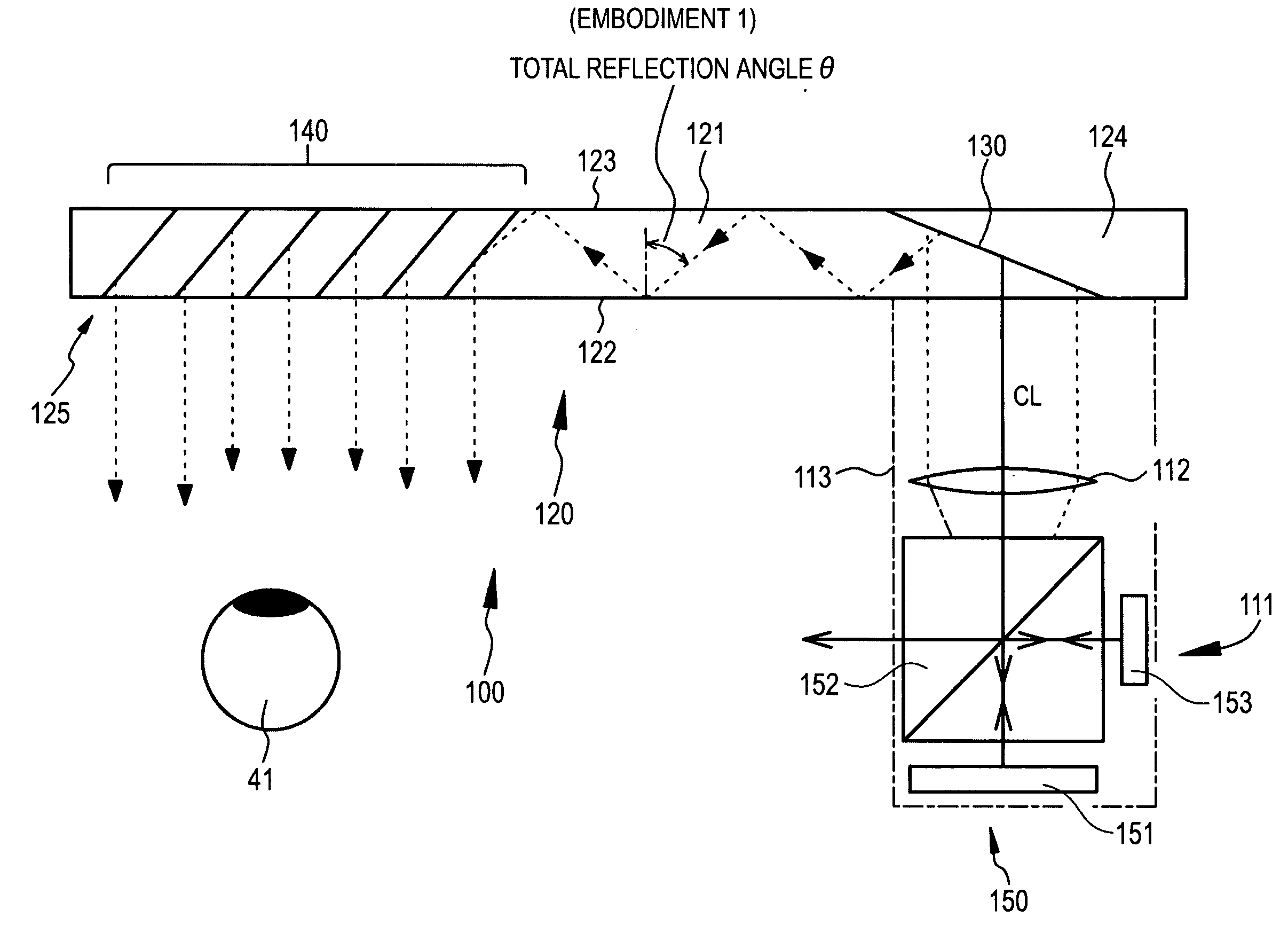
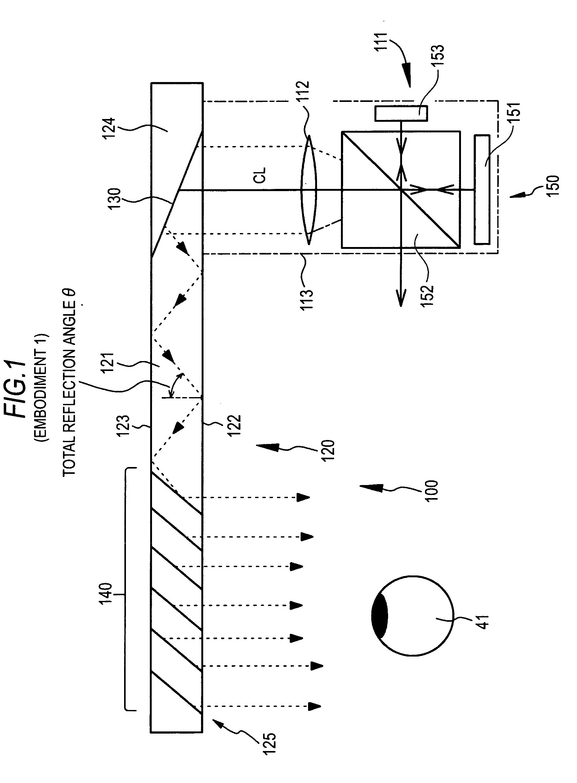
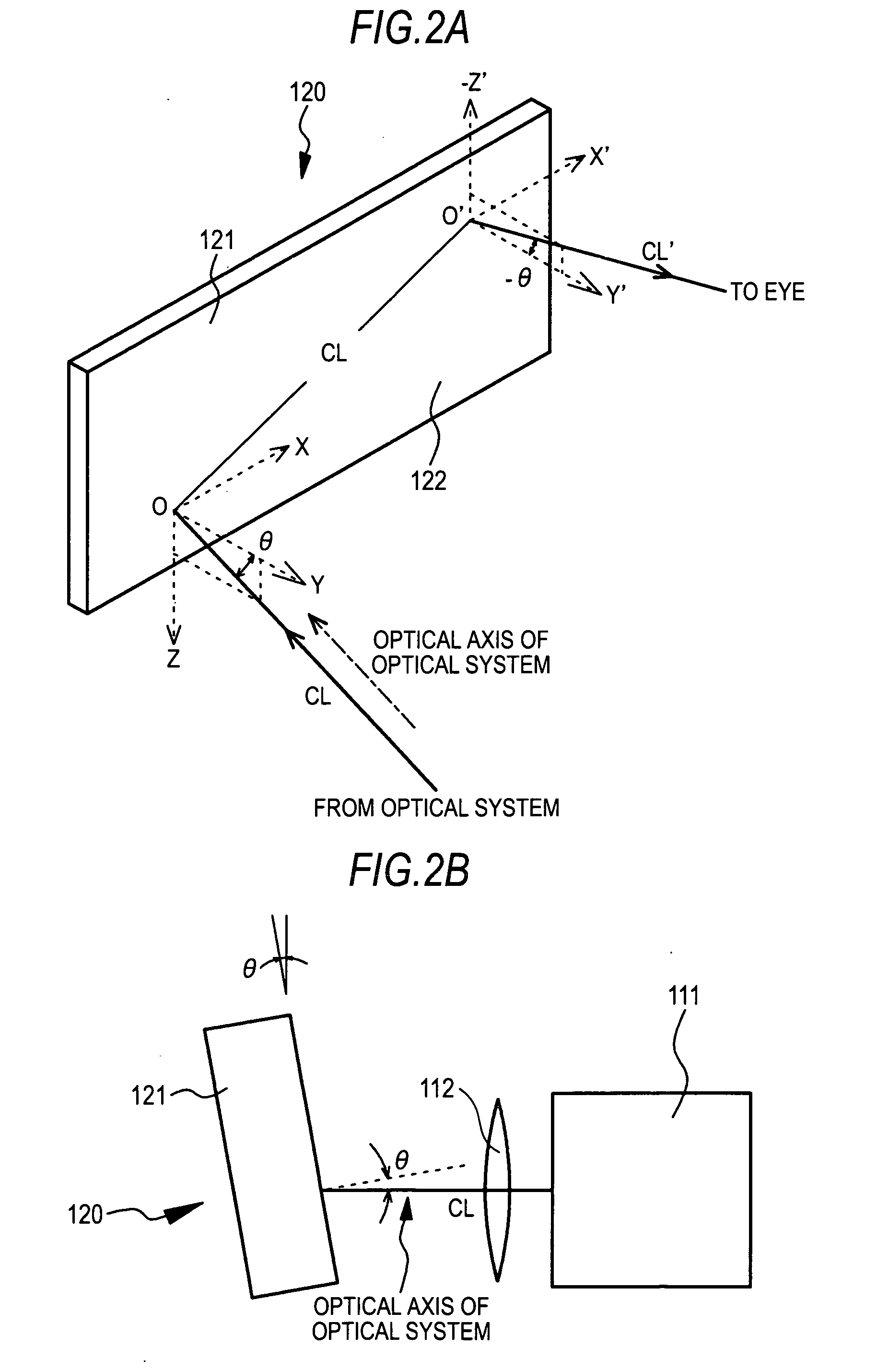
[0079]Example 1 relates to an image display apparatus according to the embodiment of the invention, and a head mounted display according to a first embodiment of the invention. A conceptual diagram of the image display apparatus of Example 1 is shown in FIG. 1, the propagation of light in alight guide plate that forms the image display apparatus of Example 1 is schematically shown in FIG. 2A, and a conceptual diagram showing an arrangement state of the light guide plate, etc. that forms the image display apparatus of Example 1 is shown in FIG. 2B. Further, a schematic view when the head mounted display of Example 1 is viewed from above is shown in FIG. 3, and a schematic view when the head mounted display is viewed from the side is shown in FIG. 4.
[0080]In Example 1 or Examples 2 to 6 that will be described below, an image display apparatus 100, 200, 300, or 400 includes:
[0081](A) an image forming device 111 or 211;
[0082](B) an optical system (parallel light emitting optical system)...
example 2
[0102]Example 2 is a modification of Example 1. FIG. 5 is a conceptual view of an image display apparatus 200 in a head mounted display according to Example 2. As shown in FIG. 5, an image forming device 211 in Example 2 is formed by an image forming device having a second configuration. That is, the image forming device includes a light source 251, and a scanning member 253 that scans the parallel light emitted from the light source 251. More specifically, the image forming device 211 includes:
[0103](a) a light source 251;
[0104](b) a collimating optical system 252 that converts light emitted from the light source 251 into parallel light;
[0105](c) a scanning member 253 that scans the parallel light emitted from the collimating optical system 252; and
[0106](d) a relay optical system 254 that relays and emits the parallel light scanned by the scanning member 253. In addition, the whole image forming device 211 is stored in a housing 213 (shown by a one-dot chain line in FIG. 5), an op...
example 3
[0109]Example 3 is also a modification of Example 1. FIG. 6A is a conceptual view of an image display apparatus 300 in a head mounted display according to Example 3. FIG. 6B is an enlarged schematic sectional view of a part of a reflective volume hologram diffraction grating. In Example 3, an image forming device 111 is formed by an image forming device having a first configuration, similarly to Example 1. An optical device 320 has the same basic configuration and structure as those of the optical device 120 of Example 1 except in the configuration and structure of a first deflecting member and a second deflecting member.
[0110]In Example 3, the first deflecting member and the second deflecting member are disposed on a surface of the light guide plate 321 (concretely, a second surface 323 of the light guide plate 321). The first deflecting member diffracts light incident on the light guide plate 321, and the second deflecting member diffracts the light, which propagates in the light ...
PUM
 Abstract
Description
Claims
Application Information
 - R&D
- Intellectual Property
- Life Sciences
- Materials
- Tech Scout
- Unparalleled Data Quality
- Higher Quality Content
- 60% Fewer Hallucinations
Browse by: Latest US Patents, China's latest patents, Technical Efficacy Thesaurus, Application Domain, Technology Topic, Popular Technical Reports.
© 2025 PatSnap. All rights reserved.Legal|Privacy policy|Modern Slavery Act Transparency Statement|Sitemap|About US| Contact US: help@patsnap.com


