Bendable X-ray sensor

a x-ray sensor and bendable technology, applied in the field of x-ray sensors, can solve the problems of low reliability, dielectric breakdown, inefficient cost and time, etc., and achieve the effect of flexible properties and effective handling of transmission targets

Active Publication Date: 2019-07-23
RAYENCE +1
View PDF34 Cites 0 Cited by
  • Summary
  • Abstract
  • Description
  • Claims
  • Application Information

AI Technical Summary

Benefits of technology

[0015]According to the present invention, in the manufacture of an X-ray sensor, the semiconductor substrate of an array substrate is removed by a predetermined thickness and is thus made thin. Therefore, the array substrate and the X-ray sensor have flexible properties, making it possible to effectively deal with transmission targets having various shapes and curvatures.

Problems solved by technology

Typically, medical or industrial X-ray imaging has been performed using films and screens, but is inefficient in terms of cost and time due to the problems of development and storage of the films used.
Since such a direct conversion X-ray sensor is operated at high voltage, it causes problems of dielectric breakdown and low reliability.
However, an indirect conversion X-ray sensor is problematic because it has a fixed shape and thus is not bendable due to the processes of forming an array element such as a light-receiving element, a transistor, etc. on a hard substrate.
Attributed to the structural limitation of such an X-ray sensor, even when the scintillator having flexible properties is used, the X-ray sensor itself does not have flexible properties.
Therefore, it is difficult to cope with various shapes and curvatures of target to be examined.

Method used


Image

  • Bendable X-ray sensor
  • Bendable X-ray sensor
  • Bendable X-ray sensor

Examples


first embodiment

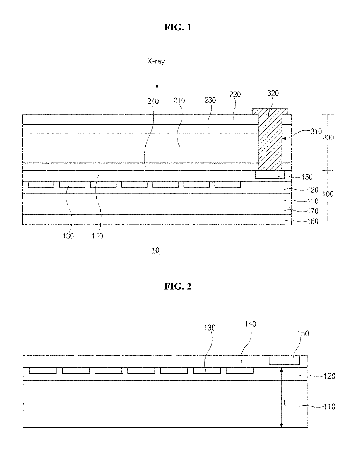
[0022]FIG. 1 is a cross-sectional view schematically illustrating an X-ray sensor according to the present invention.

[0023]As illustrated in FIG. 1, the X-ray sensor 10 according to the first embodiment of the present invention may include an array substrate 100 having light-receiving elements 130, and a scintillator panel 200 formed on a surface of the array substrate 100.

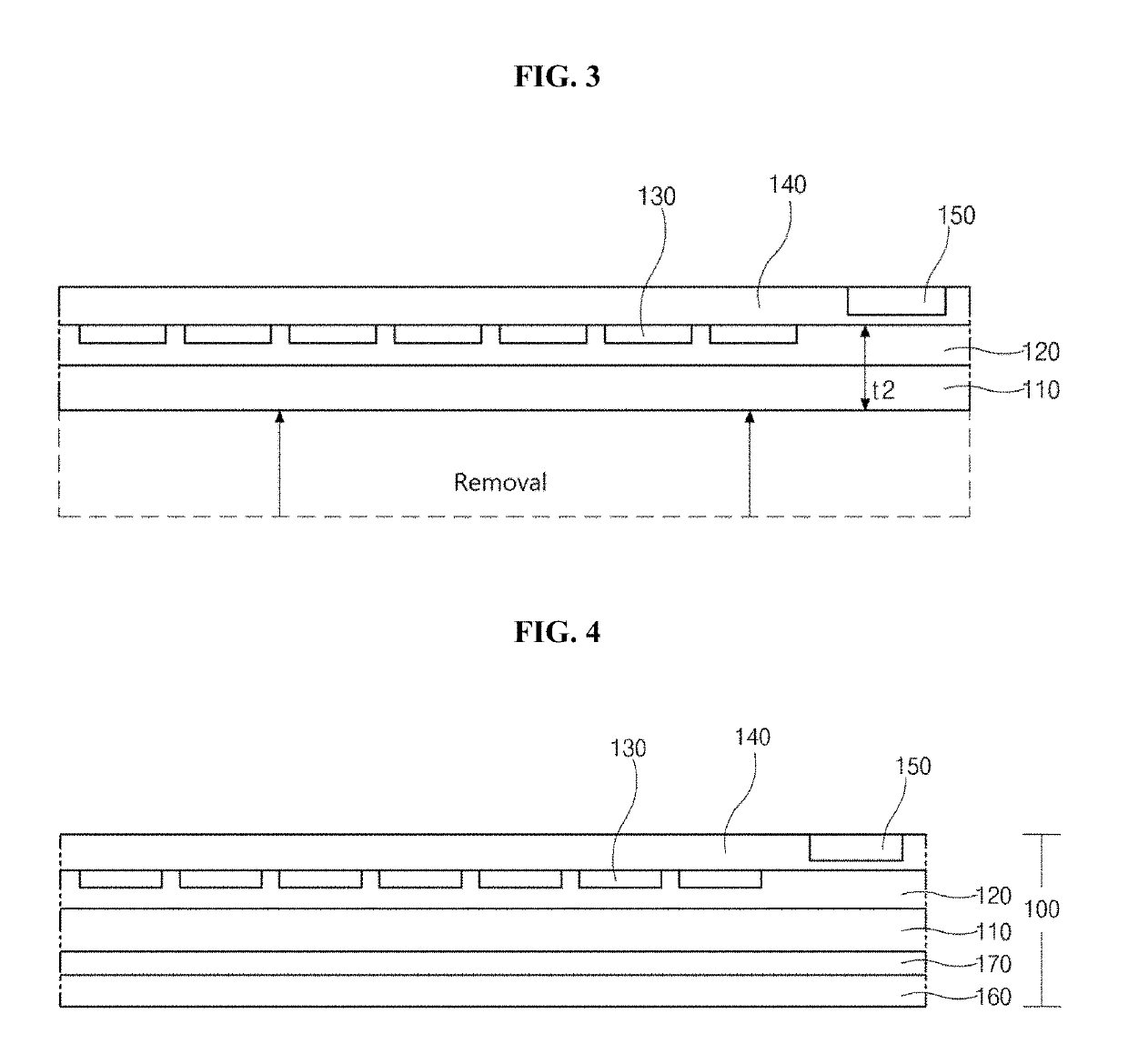
[0024]The array substrate 100 may include a semiconductor substrate 110 that is a base substrate with a semiconductor layer 120, light-receiving elements 130, a driving element layer 140, and a pad 150.

[0025]The semiconductor substrate 110 may be exemplified by a silicon substrate doped with a P type or N type impurity. In an embodiment of the present invention, for the sake of description, the use of a high concentration P+ silicon substrate is exemplified.

[0026]In the X-ray sensor 10, the rear surface of the semiconductor substrate 110 is removed by a predetermined thickness, and the semiconductor substrate 110 ...

second embodiment

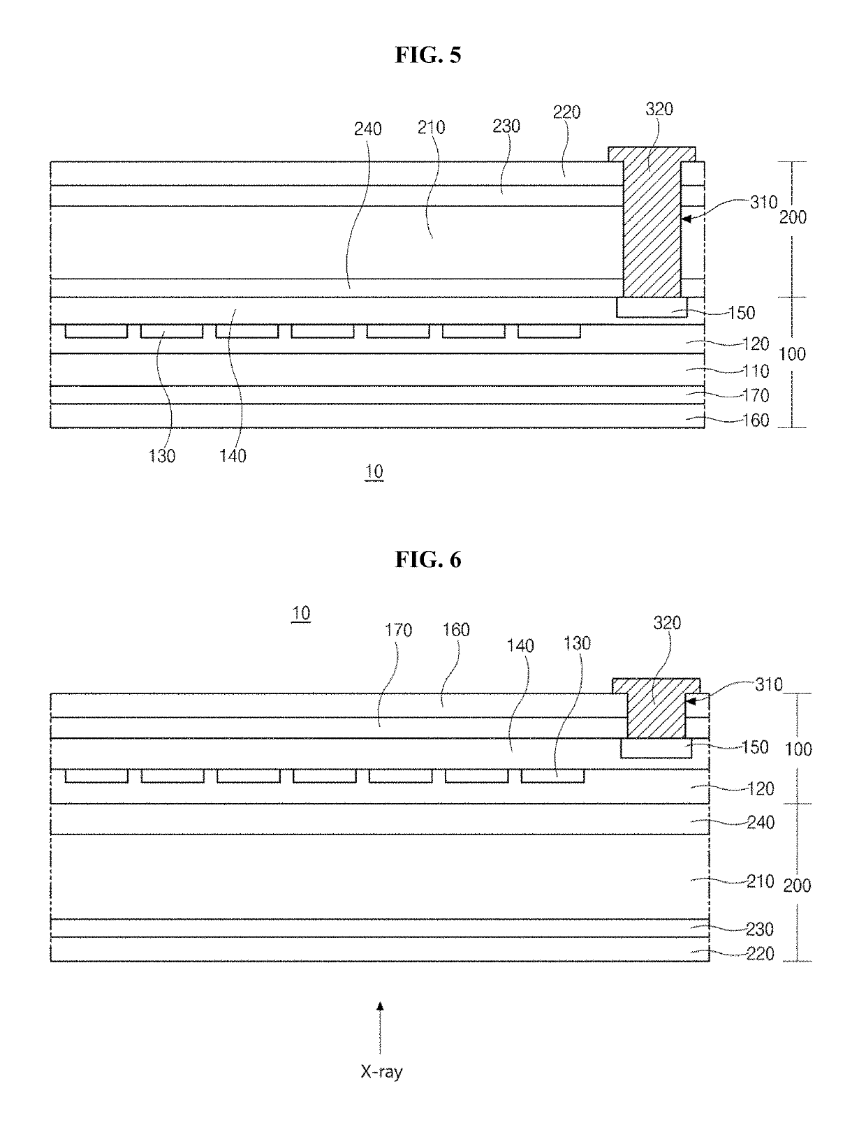
[0060]As illustrated in FIG. 6, the X-ray sensor 10 according to the present invention may include an array substrate 100 having light-receiving elements 130, and a scintillator panel 200 formed on a surface of the array substrate 100.

[0061]The array substrate 100 may include a semiconductor substrate 110 including a semiconductor layer 120, light-receiving elements 130, a driving element layer 140, and a pad 150.

[0062]The semiconductor layer 120 is formed by epitaxial growth on the upper surface of the semiconductor substrate that is used as a base substrate in the course of manufacturing the array substrate 100. The semiconductor layer 120 has the same conductive type as that of the semiconductor substrate, and may be formed of, for example, a low concentration P− type impurity.

[0063]The semiconductor substrate may be completely removed after formation of the semiconductor layer 120. Alternatively, the semiconductor substrate may be partially removed and may thus be left behind. F...


PUM


Abstract

This invention relates to an X-ray sensor having flexible properties and to a method of manufacturing the same. This X-ray sensor includes an array substrate including a semiconductor layer having a light-receiving element; a scintillator panel bonded to the array substrate and including a scintillator layer; a first polymer layer attached to an outer surface of the array substrate by a first adhesive layer; a second polymer layer attached to an outer surface of the scintillator panel by a second adhesive layer; and a third adhesive layer disposed between the array substrate and the scintillator panel so as to attach the array substrate and the scintillator panel to each other.

Description

CROSS REFERENCE TO PRIOR APPLICATIONS[0001]The present application claims priority under 35 U.S.C. § 119 to Korean Patent Application Nos. 10-2013-0118004 (filed on Oct. 2, 2013) and 10-2013-0118005 (filed on Oct. 2, 2013), which are hereby incorporated by reference in their entireties.BACKGROUND OF THE INVENTION[0002]1. Field of the Invention[0003]The present invention relates to an X-ray sensor, and more particularly, to an X-ray sensor having flexible properties and a method of manufacturing the same.[0004]2. Description of the Related Art[0005]Typically, medical or industrial X-ray imaging has been performed using films and screens, but is inefficient in terms of cost and time due to the problems of development and storage of the films used.[0006]To solve such problems, thorough research into an imaging system using a digital X-ray sensor is ongoing.[0007]An X-ray sensor may include a direct conversion X-ray sensor and an indirect conversion X-ray sensor. A direct conversion X-r...

Claims


Application Information

Patent Timeline
Patent Type & Authority Patents(United States)
IPC IPC(8): H01L27/146H01L27/30G01T1/24G01T1/20G21K4/00H01L31/08
CPCH01L27/14663G01T1/20G01T1/2002G01T1/2018G01T1/24H01L27/14601H01L27/14625H01L27/14685H01L27/308G21K4/00H01L31/085G01T1/20189H10K39/36
Inventor HEO, SUNG KYNLEE, HO SEOK
Owner RAYENCE
Why Eureka
Try Eureka