
Semiconductor device including clock generating circuit and channel management circuit

a technology of semiconductor circuits and semiconductor devices, applied in the direction of generating/distributing signals, instruments, high-level techniques, etc., can solve problems such as soc malfunctions or soc damag

Active Publication Date: 2019-04-02
SAMSUNG ELECTRONICS CO LTD
View PDF79 Cites 1 Cited by
  • Summary
  • Abstract
  • Description
  • Claims
  • Application Information

AI Technical Summary

Benefits of technology

This solution effectively reduces power consumption by ensuring that only necessary components are active, thereby minimizing heat generation and preventing damage, while maintaining normal operation during active states and reducing power usage in standby modes.

Problems solved by technology

As SoCs increase in integration density and size, and as the operating speed thereof is improved, low power consumption becomes an important factor, since high power consumption may raise the temperature of a chip, resulting in the SoC malfunctioning or the SoC being damaged.

Method used


Image

  • Semiconductor device including clock generating circuit and channel management circuit
  • Semiconductor device including clock generating circuit and channel management circuit
  • Semiconductor device including clock generating circuit and channel management circuit

Examples


Embodiment Construction

[0029]It will be understood that the terms “first,”“second,”“third,” etc. are used herein to distinguish one element from another, and the elements are not limited by these terms. Thus, a “first” element in an exemplary embodiment may be described as a “second” element in another exemplary embodiment.

[0030]Further, when two processes are described as being performed substantially simultaneously or at substantially the same time as each other, it is to be understood that the processes may be performed at exactly the same time or at about the same time as would be understood by a person having ordinary skill in the art.

[0031]Further, it will be understood that each of the units described herein may be implemented as and referred to as circuits (e.g., a clock MUX unit be implemented as a circuit and referred to as a clock MUX circuit, a clock gating unit may be implemented as a circuit and referred to as a clock gating circuit, a channel management unit may be implemented as a circuit ...


PUM


Abstract

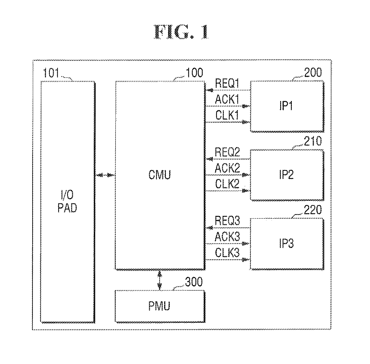
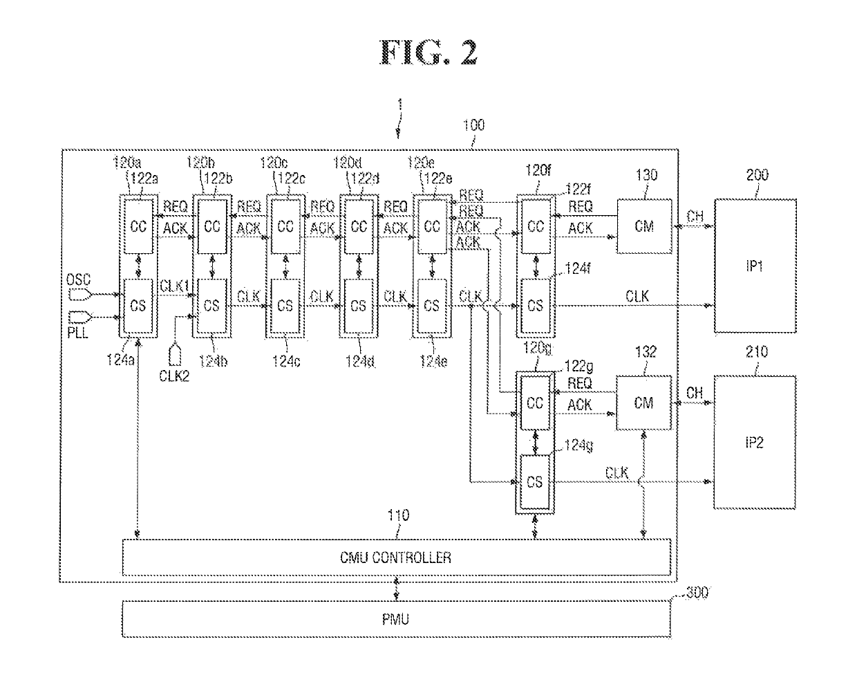
A semiconductor device includes a first clock generating circuit including a first control circuit and a first clock gating circuit, a first channel management circuit which communicates with the first clock generating circuit according to a full handshake method, a second clock generating circuit including a second control circuit and a second clock gating circuit, and a second channel management circuit which communicates with the second clock generating circuit according to the full handshake method. The first clock gating circuit outputs a first clock, and the second clock gating circuit outputs a second clock different from the first clock.

Description

CROSS-REFERENCE TO RELATED APPLICATIONS[0001]This application claims priority to and the benefit of U.S. Provisional Patent Application No. 62 / 286,895 filed on Jan. 25, 2016, U.S. Provisional Patent Application No. 62 / 286,860 filed on Jan. 25, 2016, Korean Patent Application No. 10-2017-0007002 filed on Jan. 16, 2017, and Korean Patent Application No. 10-2017-0010945 filed on Jan. 24, 2017, the disclosures of which are incorporated by reference herein in their entireties.TECHNICAL FIELD[0002]Exemplary embodiments of the present disclosure relate to a semiconductor device including a semiconductor circuit.DISCUSSION OF THE RELATED ART[0003]With the gradual convergence of computers, communications, broadcasts, etc., the demand for existing application specific integrated circuits (ASICs) and application specific standard products (ASSPs) is changing due to the demand for system-on-chips (SoCs). Further, the trend toward lighter, thinner, more compact and high-performance information t...

Claims


Application Information

Patent Timeline
Patent Type & Authority Patents(United States)
IPC IPC(8): G06F1/00H04L5/00G06F1/06G06F1/3237
CPCG06F1/06G06F1/3237Y02D50/20Y02D10/128Y02D10/00Y02D30/50
Inventor KIM, SE HUNKIM, AH CHANCHOI, YOUN SIKLEE, JAE GON
Owner SAMSUNG ELECTRONICS CO LTD
Learn More