Method for positioning a carrier with electronic components and electronic component produced with such method

a technology of electronic components and positioning methods, which is applied in the direction of semiconductor/solid-state device testing/measurement, semiconductor device details, semiconductor/solid-state device testing/measurement, etc., can solve the problems of higher rejection levels, and achieve the effect of increasing detection feasibility and improving detection quality of solder mask shi

Active Publication Date: 2019-02-26
BESI NETHERLANDS BV
View PDF13 Cites 0 Cited by
  • Summary
  • Abstract
  • Description
  • Claims
  • Application Information

AI Technical Summary

Benefits of technology

The patent text describes a method for improving the accuracy of wiring detection on semiconductor carriers and improving the overall accuracy of the process. By detecting and correcting any inaccuracy in the positioning of solder mask or bus lines, the method ensures better quality products and reduces the likelihood of rejections. The use of co-axial lighting also enhances the detection of solder mask shift.

Problems solved by technology

In case of inaccuracy in the positioning of these “bus lines” later isolation of the semiconductors could be frustrated leading to higher rejection levels.

Method used


Image

  • Method for positioning a carrier with electronic components and electronic component produced with such method
  • Method for positioning a carrier with electronic components and electronic component produced with such method
  • Method for positioning a carrier with electronic components and electronic component produced with such method

Examples


Embodiment Construction

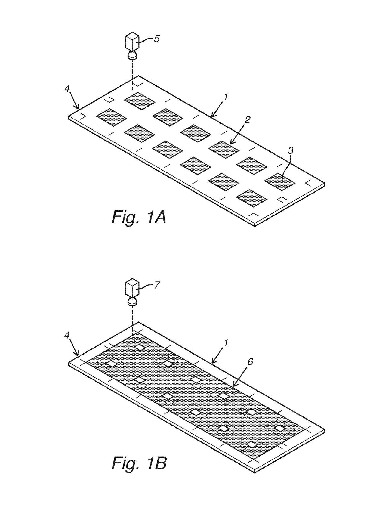
[0020]FIG. 1A shows a perspective view on carrier 1 which is provided from a pattern 2 of wiring and contact pads (seen only in general and indicated by the grey area's 3). On the carrier 1 are also carrier related references 4 that are often affixed together with the wiring and contact pads. In FIG. 1A is also shown that a vision camera 5 detects the carrier related references 4.

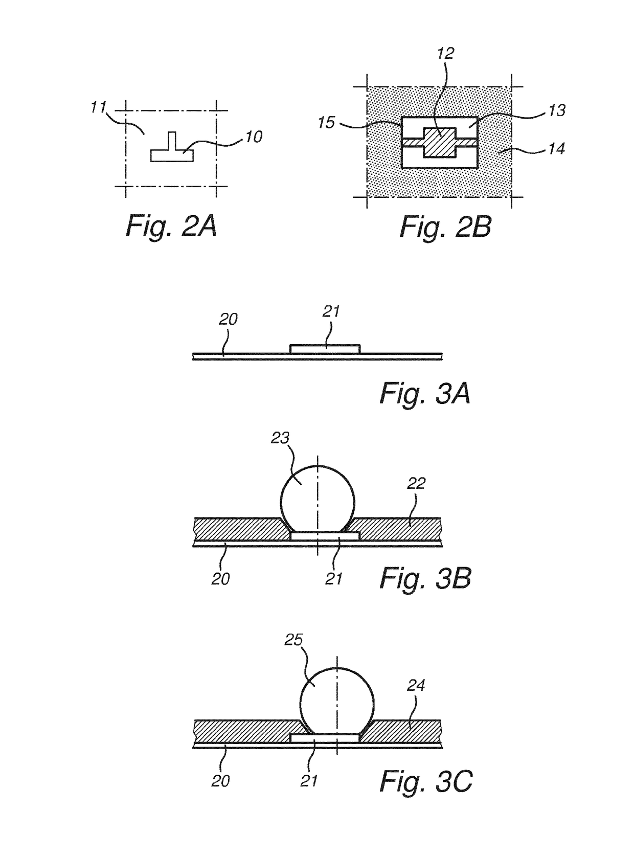
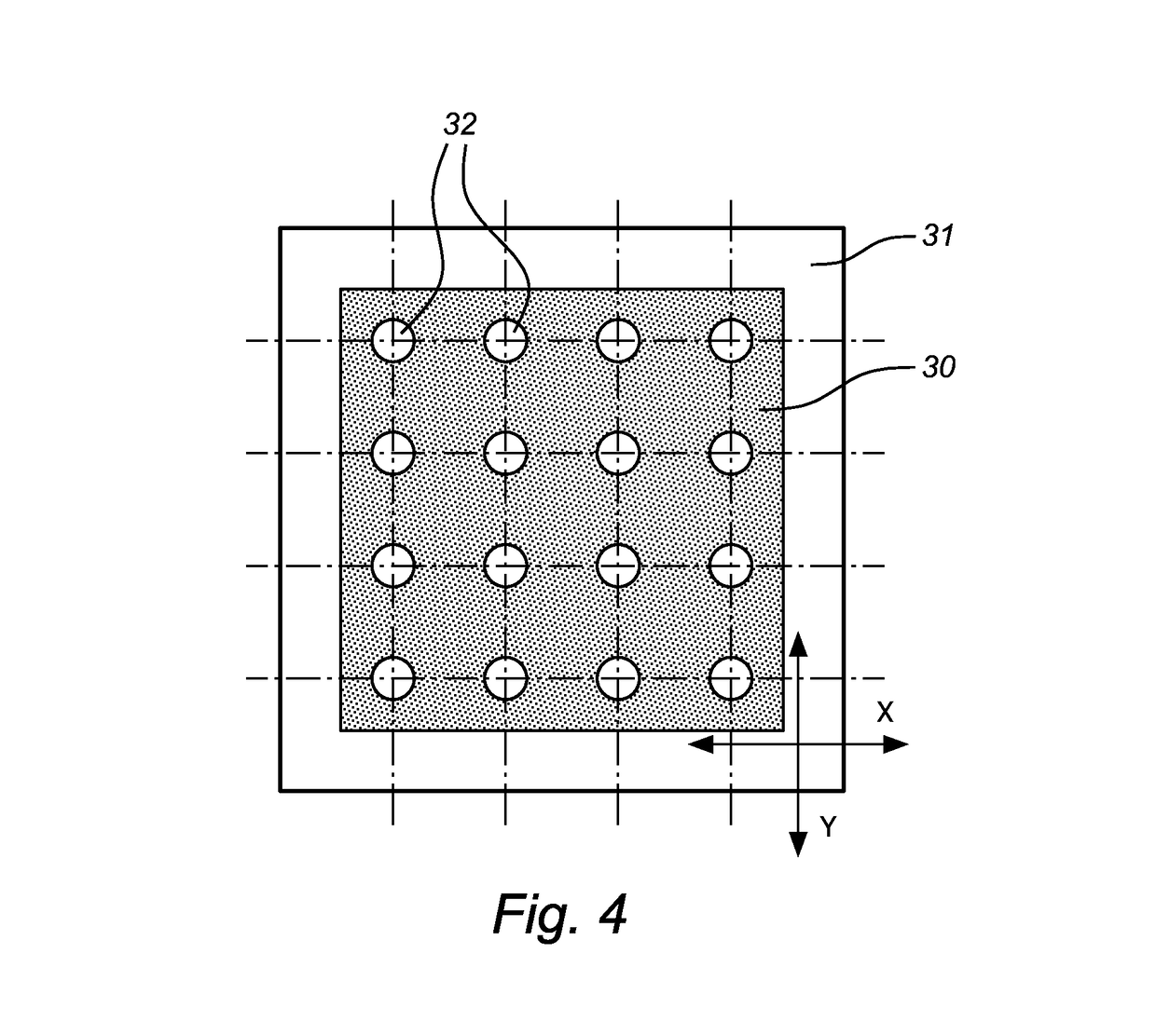
[0021]FIG. 1B shows a perspective view on the carrier 1 from FIG. 1A but now after a solder mask 6 has been added to the carrier 1 leaving locally only minor openings free to enable the placing of contacts as will be explained in connection to FIGS. 3A-3C and 4. In FIG. 1B again a vision camera 7 is shown now for the detection of solder mask dependent references as will be explained in connection to FIG. 2B. In stead of detecting the carrier related references 4 before the solder mask 6 has been added to the carrier 1 the present invention also covers the detection of the carrier related references 4 after ...


PUM


Abstract

The present invention relates to a method of processing a solder masked carrier with electronic components, comprising the detection of a carrier related reference and the detection of a solder mask dependent reference, which detected reference are used for processing the position of the solder mask on the carrier. The invention also relates to an electronic component as produced with such method.

Description

CROSS-REFERENCE TO RELATED APPLICATIONS[0001]This application is the United States national phase of International Application No. PCT / NL2014 / 050702 filed Oct. 8, 2014, which claims priority to Dutch Application No. 2011575 filed Oct. 8, 2013, the disclosures of which are hereby incorporated in their entirety by reference.BACKGROUND OF THE INVENTIONField of the Invention[0002]The invention relates to a method of processing a carrier with electronic components, comprising the method steps: detecting at least one carrier related reference; processing the at least one detected carrier related reference into a position of the carrier and processing the solder masked carrier with electronic components. The invention also relates to an electronic component produced with such a method.Description of Related Art[0003]The manufacturing electronic components, such as more particularly—but not exclusively—semiconductor products, usually takes place in larger quantities by making use of units o...

Claims


Application Information

Patent Timeline
Patent Type & Authority Patents(United States)
IPC IPC(8): H01L23/00H01L21/66H01L21/48H01L23/544H01L21/78H01L23/498
CPCH01L22/22H01L21/4853H01L21/78H01L22/30H01L23/544H01L2924/0002H01L23/49816H01L2223/5442H01L2223/54426H01L2223/54453H01L2223/54486H01L2224/03013H01L2224/73253H01L2924/00H01L2924/0001
Inventor HUISSTEDE, JURGEN HENDRIKUS GERHARDUSHERMANS, MARK
Owner BESI NETHERLANDS BV
Why Eureka
Try Eureka