
Semiconductor memory device and reading method thereof

a memory device and semiconductor technology, applied in the direction of digital storage, static storage, instruments, etc., can solve the problems of longer time required for charging/discharging bit lines, longer time for reading data, etc., and achieve the effect of suppressing peak current and noise and preventing power voltag

Active Publication Date: 2018-11-27
WINBOND ELECTRONICS CORP
View PDF8 Cites 3 Cited by
  • Summary
  • Abstract
  • Description
  • Claims
  • Application Information

AI Technical Summary

Benefits of technology

This approach effectively suppresses peak current and noise during bit line pre-charging, ensuring stable power voltage and preventing operational failures, especially in low power devices.

Problems solved by technology

When a resistance of the bit line becomes higher due to miniaturization and a capacitance of the bit line increases due to an increasing number of pages, a time required for charging / discharging the bit line becomes longer so it will take longer to read data.

Method used


Image

  • Semiconductor memory device and reading method thereof
  • Semiconductor memory device and reading method thereof
  • Semiconductor memory device and reading method thereof

Examples


Embodiment Construction

[0018]Reference will now be made in detail to the present preferred embodiments of the invention, examples of which are illustrated in the accompanying drawings. Wherever possible, the same reference numbers are used in the drawings and the description to refer to the same or like parts.

[0019]Embodiments of the invention are described in detail below by reference with accompanied figures. Methods for suppressing the power voltage from dropping when pre-charging include a layout-related method such as separating wiring for the power, a circuit-related method such as inserting a resistor into a power source, etc. In the present embodiment, a logic sequence control is used as the method for suppressing the peak current noise.

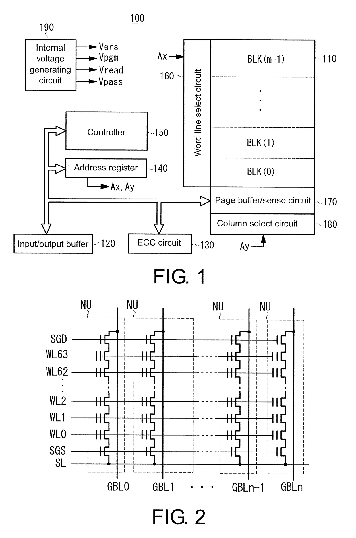
[0020]FIG. 1 is a diagram illustrating a structure of an NAND flash memory according to an embodiment of the invention. A flash memory 100 of the present embodiment includes: a memory array 110, formed by a plurality of memory cells arranged in matrix; an input / out...


PUM


Abstract

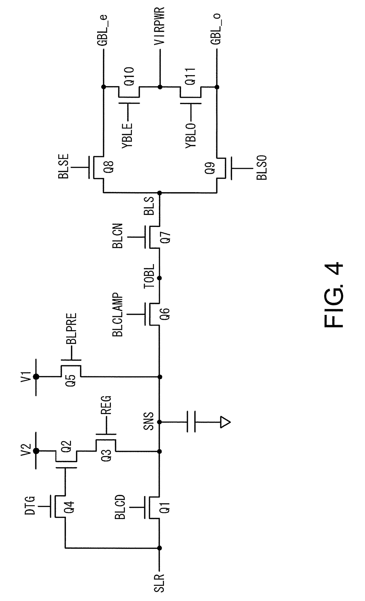
The invention provides a semiconductor memory device and a reading method thereof, which are capable of suppressing a peak current when pre-charging a bit line are provided. The reading method of a flash memory of the present invention includes steps of: pre-charging a selected bit line; and reading a voltage or a current of the pre-charged selected bit line. The step of pre-charging is performed by pre-charging a sense node SNS to Vcc−Vth at a time t1, pre-charging a node TOBL to VCLAMP2 at a time t2, pre-charging the node TOBL to VCLAMP1 at a time t5, and pre-charging the sense node SNS to Vcc at a time t6.

Description

CROSS-REFERENCE TO RELATED APPLICATION[0001]This application claims the priority benefit of Japan application serial no. 2016-163324, filed on Aug. 24, 2016. The entirety of the above-mentioned patent application is hereby incorporated by reference herein and made a part of this specification.BACKGROUND OF THE INVENTION1. Field of the Invention[0002]The invention relates to a reading of a semiconductor storage device, such as an NAND flash memory, and more particularly, to a pre-charging of a bit line.2. Description of Related Art[0003]When reading pages in the NAND flash memory, a page buffer / sense circuit is used to pre-charge a bit line, and the bit line is discharged according to a storage state of a selected memory cell. Later, a potential or a current of the bit line is sensed at a sense node. When a resistance of the bit line becomes higher due to miniaturization and a capacitance of the bit line increases due to an increasing number of pages, a time required for charging / dis...

Claims


Application Information

Patent Timeline
Patent Type & Authority Patents(United States)
IPC IPC(8): G11C16/06G11C29/52G11C16/24G11C16/04G11C7/02G11C11/413G11C7/14G11C7/18G11C7/12G11C29/04
CPCG11C7/12G11C7/02G11C7/14G11C7/18G11C16/0483G11C16/24G11C29/52G11C11/413G11C2207/005G11C2029/0411G11C16/26G11C16/30G11C29/42
Inventor YAMAUCHI, KAZUKI
Owner WINBOND ELECTRONICS CORP
Learn More