Thin film transistor substrate and display using the same
a technology of thin film transistors and substrates, applied in the direction of electrical equipment, semiconductor devices, instruments, etc., can solve the problems of limiting the availability of display substrates with excellent low power consumption properties, and achieve the effect of low frequency driving characteristics and low power consumption properties
- Summary
- Abstract
- Description
- Claims
- Application Information
AI Technical Summary
Benefits of technology
Problems solved by technology
Method used
Image
Examples
first embodiment
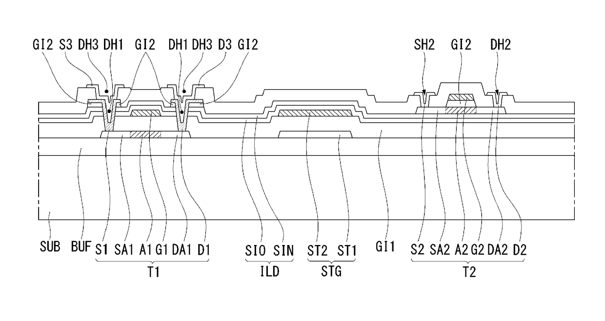
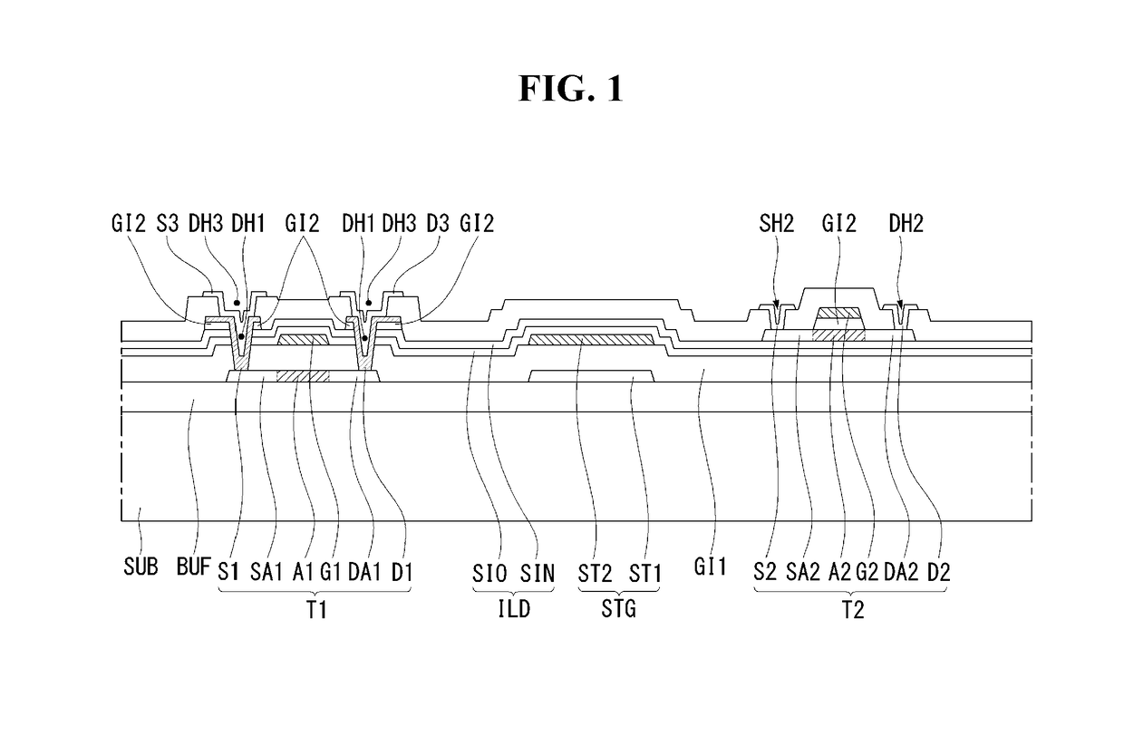
[0044]Referring to FIG. 1, we will explain about the first embodiment of the present disclosure. FIG. 1 is a cross sectional view illustrating a structure of a thin film transistor substrate for a flat panel display in which two different type thin film transistors are formed, according to the first embodiment of the present disclosure. Here, we will explain with the cross sectional views mainly because it clearly shows the main features of the present disclosure, in convenience, the plane view is not used.
[0045]Referring to FIG. 1, the thin film transistor substrate for a flat panel display according to the first embodiment comprises a first thin film transistor T1 and a second thin film transistor T2 which are disposed on the same substrate SUB. The first and second thin film transistors T1 and T2 may be apart far from each other, or they may be disposed within a relatively closed distance. Otherwise these two thin film transistors are disposed as being overlapped each other.
[0046...
second embodiment
[0083]Hereinafter, referring to FIG. 3, we will explain about the second embodiment of the present disclosure. FIG. 3 is a cross sectional view illustrating a structure of a thin film transistor substrate for a flat panel display in which two different type thin film transistors are formed, according to the second embodiment of the present disclosure.
[0084]The thin film transistor substrate according to the second embodiment is basically very similar with that of the first embodiment. The main difference is on a first light shielding layer LS1 for preventing the lights from the outside of the bottom side of the first thin film transistor T1. Further, under the second thin film transistor T2, a second light shielding layer LS2 may be further included for preventing the light incident from outside.
[0085]The first light shielding layer LS1 may be formed by separated mask process, under the buffer layer BUF. The second light shielding layer LS2 may be formed of the same material and at ...
first application example
[0101]The thin film transistor substrate having two different type thin film transistors on the same substrate, above explained, can be applied to various type display including the flat panel display, the flexible display and / or the curved display. Forming the different two type thin film transistors on the same substrate, we can get various merits. Hereinafter, referring to FIG. 5, we will explain how many advanced features and merits can be expected from the thin film transistor substrate according to a first application example of the present disclosure. FIG. 5 is a block diagram illustrating a structure of the display according to a first application example of the present disclosure.
[0102]The first and the second transistors T1 and T2 would be formed in each pixel of the display panel 100 for switching the data voltage applied to the pixel or for driving the pixel. For the case of organic light emitting diode display, the second thin film transistor T2 may be a switch element ...
PUM
| Property | Measurement | Unit |
|---|---|---|
| temperature | aaaaa | aaaaa |
| frequency | aaaaa | aaaaa |
| shape | aaaaa | aaaaa |
Abstract
Description
Claims
Application Information
 - R&D
- Intellectual Property
- Life Sciences
- Materials
- Tech Scout
- Unparalleled Data Quality
- Higher Quality Content
- 60% Fewer Hallucinations
Browse by: Latest US Patents, China's latest patents, Technical Efficacy Thesaurus, Application Domain, Technology Topic, Popular Technical Reports.
© 2025 PatSnap. All rights reserved.Legal|Privacy policy|Modern Slavery Act Transparency Statement|Sitemap|About US| Contact US: help@patsnap.com


