Liquid crystal display device

a display device and liquid crystal technology, applied in static indicating devices, instruments, non-linear optics, etc., can solve the problems of deterioration of the response characteristics to voltage and the orientation of liquid crystal molecules, and achieve the effect of high dielectric material layer

Active Publication Date: 2018-11-06
SATURN LICENSING LLC
View PDF30 Cites 2 Cited by
  • Summary
  • Abstract
  • Description
  • Claims
  • Application Information

AI Technical Summary

Benefits of technology

[0034]According to the liquid crystal display device in the first mode of the present disclosure, the first transparent conductive material layer connected to the first power supply portion is formed on the protrusion top faces of the base layer, while the second transparent conductive material layer connected to the second power supply portion is formed on the recess bottom faces of the base layer. The first transparent conductive material layer and the second transparent conductive material layer are separated from each other. That is, in this case, a certain type of edge portion is formed at a portion of the first transparent conductive material layer separated from the second transparent conductive material layer. Therefore, the presence of the certain type of edge portion formed on the first transparent conductive material layer increases the intensity of the electric field generated at the protrusions of the base layer at a portion of the first electrode to orient the liquid crystal molecules, particularly the liquid crystal molecules in the vicinity of the side of the base layer in response to application of voltage to the first electrode. Moreover, an electric field profile thus produced becomes uniform. Furthermore, according to the liquid crystal display devices in the second and the third modes of the present disclosure, the high dielectric material layer is provided. In this case, an electric field profile produced by the first electrode and the second electrode becomes uniform. In addition, light transmittance of the liquid crystal layer becomes uniform in accordance with the uniformity of the electric field profile. Note that advantageous effects described in the present specification are presented only by way of example. Advantageous effects described in the present specification are not limited to the advantageous effects described herein, and may include additional effects.

Problems solved by technology

This randomness of the falling directions may cause disorder of the orientation of the liquid crystal molecules, and deteriorate response characteristics to voltage.

Method used


Image

  • Liquid crystal display device
  • Liquid crystal display device
  • Liquid crystal display device

Examples


first embodiment

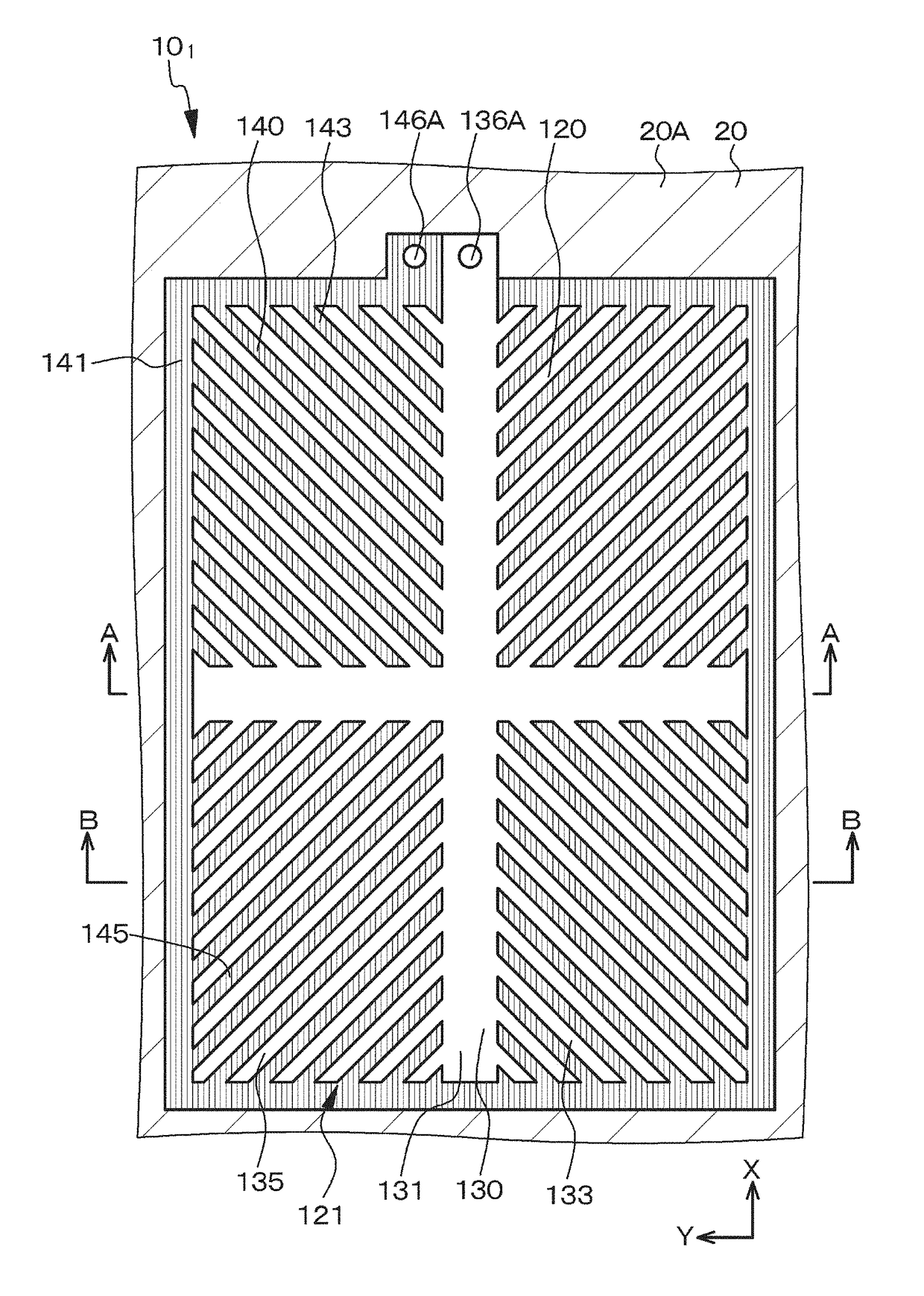
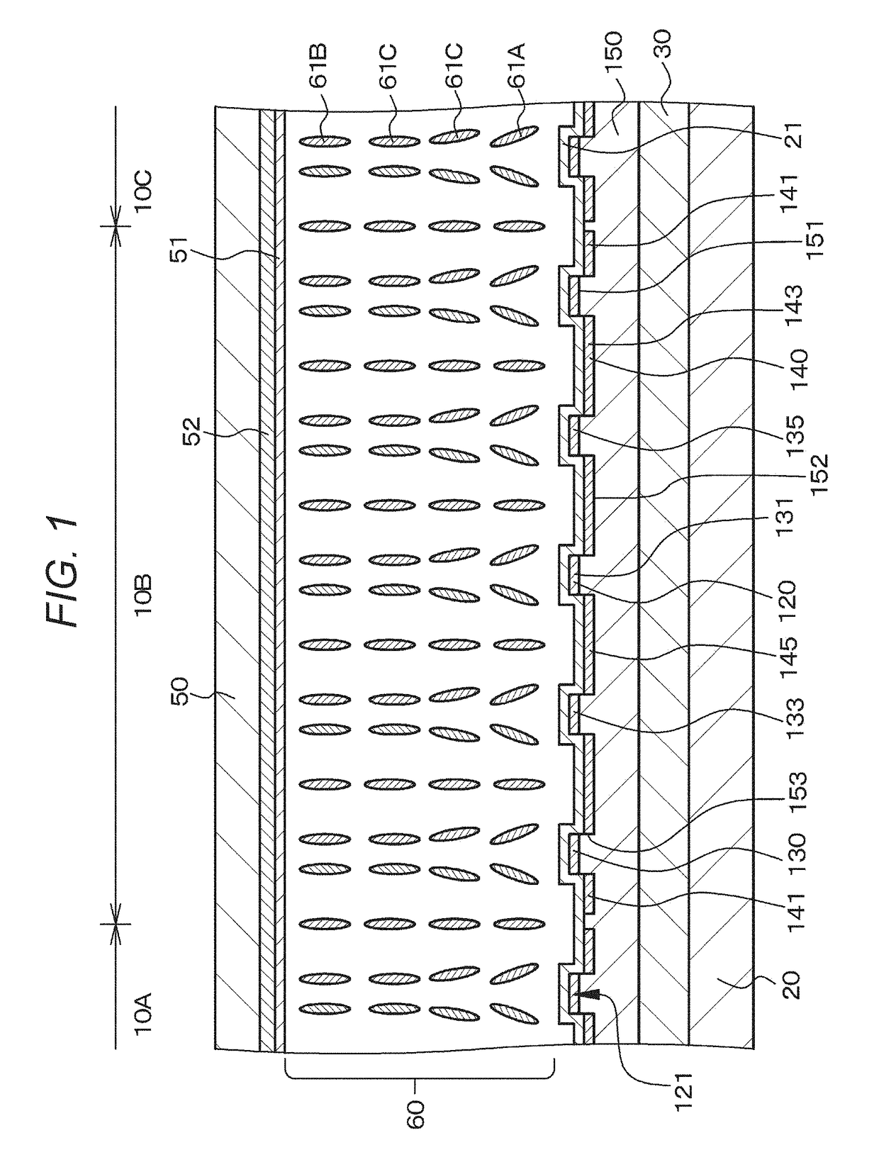
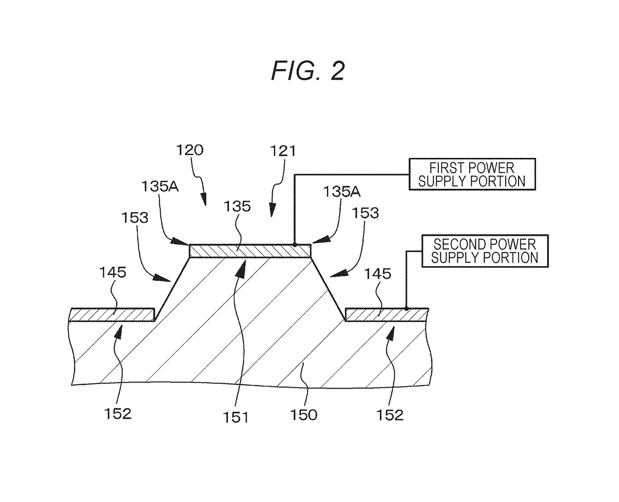
[0213]A first embodiment relates to a liquid crystal display device in the first mode of the present disclosure, more specifically, a liquid crystal display device in a first example of the first mode. FIG. 1 illustrates a schematic partial cross-sectional view of the liquid crystal display device according to the first embodiment. FIG. 2 is a schematic partial end face view showing an enlarged part of recesses and protrusions of a base layer, a first transparent conductive material layer, and a second transparent conductive material layer. FIG. 3 is a schematic view of one pixel 101 on a first substrate 20 as viewed from above. FIG. 8A is a schematic end face view taken along an arrow A-A in FIG. 3. FIG. 8B is a schematic end face view taken along an arrow B-B in FIG. 3. FIG. 8C is a schematic partial end face view of an enlarged part illustrated in FIG. 8B.

[0214]The liquid crystal display device according to the first embodiment, or each of liquid crystal display devices according...

second embodiment

[0296]The second embodiment is a modification of the first embodiment, and relates to the liquid crystal display device in the second example of the first mode. FIG. 9 is a schematic view of one pixel 102 on the first substrate 20 constituting the liquid crystal display device of the second embodiment as viewed from above. FIG. 11A is a schematic end face view taken along an arrow A-A in FIG. 9, while FIG. 11B is a schematic end face view taken along an arrow B-B in FIG. 9. While the liquid crystal display device in the second embodiment illustrated in FIG. 9 is a modification of the liquid crystal display device in the first embodiment illustrated in FIG. 3, the liquid crystal display device in the second embodiment may have other configurations, such as a modification of the liquid crystal display device of the first embodiment illustrated in FIG. 4.

[0297]In the liquid crystal display device according to the second embodiment,

[0298]protrusions 230 are constituted by the stem protr...

third embodiment

[0302]The third embodiment is a modification of the liquid crystal display devices of the first and second examples of the first mode. Each of FIGS. 12 and 13 is a schematic partial end face view of a liquid crystal display device according to the third embodiment. In addition, each of FIGS. 51B and 51C is a conceptual view illustrating a behavior of liquid crystal molecules in the liquid crystal display device according to the third embodiment.

[0303]According to the liquid crystal display device of the third embodiment, the stem protrusion 131 passing through a pixel central portion and extending radially (e.g. in cross shape) (more specifically, extending in parallel with X axis and Y axis, for example) is formed on the first electrode 120 similarly to the first embodiment. In addition, an orientation regulation portion 53 is formed in a portion of the second electrode 52 corresponding to the stem protrusion 131 as illustrated in FIG. 12 or 13.

[0304]More specifically, the orientat...


PUM

PropertyMeasurementUnit
dielectric constantaaaaaaaaaa

Abstract

A liquid crystal display device includes a plurality of arranged pixels. Each of the pixels includes: a first substrate and a second substrate; a first electrode provided on a counter face of the first substrate, the counter face facing the second substrate; a second electrode provided on a counter face of the second substrate, the counter face facing the first substrate; and a liquid crystal layer that contains liquid crystal molecules, and is sandwiched between the first substrate and the second substrate. The liquid crystal molecules are given a pre-tilt. The first electrode includes a base layer 150 that contains a plurality of recesses and protrusions, and transparent conductive material layers 135 and 145. The first transparent conductive material layer 135 connected to a first power supply portion is formed on protrusion top faces 151 of the base layer 150. The second transparent conductive material layer 145 connected to a second power supply portion is formed on recess bottom faces 152 of the base layer 150. The first transparent conductive material layer 135 and the second transparent conductive material layer 145 are separated from each other.

Description

CROSS REFERENCE TO RELATED APPLICATIONS[0001]This application is a U.S. National Phase of International Patent Application No. PCT / JP2016 / 054549 filed on Feb. 17, 2016, which claims priority benefit of Japanese Patent Application No. JP 2015-058588 filed in the Japan Patent Office on Mar. 20, 2015. Each of the above-referenced applications is hereby incorporated herein by reference in its entirety.TECHNICAL FIELD[0002]The present disclosure relates to a liquid crystal display device provided with a liquid crystal display element which includes a liquid crystal layer sealed between a pair of substrates.BACKGROUND ART[0003]In recent years, a liquid crystal display device (liquid crystal display (LCD)) has been widely used to provide a display monitor for a liquid crystal television receiver, a laptop, a car navigation device and the like. This type of liquid crystal display device is classified into various types of display modes (systems) on the basis of molecular arrangement (orient...

Claims


Application Information

Patent Timeline
Patent Type & Authority Patents(United States)
IPC IPC(8): G02F1/1345G02F1/1343G02F1/1335G09G3/18
CPCG02F1/1343G02F1/133512G02F1/133514G02F1/133602G09G3/18G02F1/133528G09G2310/0264G02F1/133371G02F1/133707G02F1/134363G09G3/3648
Inventor SUWA, SHUNICHIMIYAKAWA, MASASHIKOBAYASHI, CHIKASHINAGASE, YOJINAGAMINE, KUNIHIKO
Owner SATURN LICENSING LLC
Why Eureka
Try Eureka