
Driver circuit and semiconductor module having same

a driver circuit and semiconductor technology, applied in the direction of pulse technique, process and machine control, instruments, etc., can solve the problems of high impedance between the source of the main switch and the low-voltage side power supply terminal of the driver circuit, and the main switch is more prone to erroneous switching on or off, so as to suppress the rapid change of current (di/dt), increase the resistance of a current limiting resistor, and prevent extremely large currents

Active Publication Date: 2018-08-28
FUJI ELECTRIC CO LTD
View PDF6 Cites 3 Cited by
  • Summary
  • Abstract
  • Description
  • Claims
  • Application Information

AI Technical Summary

Benefits of technology

[0014]Adding the current limiting resistor (RR) connects together the source of the main switch and the low-voltage side power supply terminal of the driver circuit via the current limiting resistor (RR). Therefore, even if the source voltage becomes a lower voltage than the reference voltage of the driver circuit due to parasitic inductance on the source side of the main switch and due to a rapid change in current (−di / dt) when the main switch switches OFF, the current limiting resistor (RR) makes it possible to reduce the current flowing from the reference voltage of the driver circuit to the source of the main switch via the low-voltage side power supply line of the driver circuit.
[0015]This, in turn, makes it possible to suppress the flow of current from the low-side power supply of the driver circuit to the source of the main switch when the source takes a negative voltage.
[0019]Accordingly, the present invention is directed to a scheme that substantially obviates one or more of the problems due to limitations and disadvantages of the related art. In particular, in some embodiments, the present invention aims to provide a driver circuit that, without having to excessively increase the resistance of a current limiting resistor (RR), suppresses the rapid changes in current (di / dt) accompanying switching of a power semiconductor device and also prevents excessively large currents resulting from such rapid changes (di / dt) from occurring in a low-voltage side power supply line of the driver circuit. Moreover, the present invention aims to provide a semiconductor module including such a driver circuit.
[0027]The driver circuit according to the present invention makes it possible to, without having to excessively increase the resistance of a current limiting resistor, suppress the rapid changes in current (di / dt) accompanying switching of a power semiconductor device such as an IGBT or a MOSFET and also prevent extremely large currents resulting from such rapid changes (di / dt) from occurring in a low-voltage side power supply line of the driver circuit. It is to be understood that both the foregoing general description and the following detailed description are exemplary and explanatory, and are intended to provide further explanation of the invention as claimed.

Problems solved by technology

(1) When the resistance of the current limiting resistor (RR) is set to a large value, the impedance between the source of the main switch and the low-voltage side power supply terminal of the driver circuit becomes high regardless of whether the main switch is ON or OFF. As a result, the main switch is more prone to erroneously switching ON or OFF due to other switches (not illustrated in the figure) in the driver circuit switching ON and OFF or due to external noise.

Method used


Image

  • Driver circuit and semiconductor module having same
  • Driver circuit and semiconductor module having same
  • Driver circuit and semiconductor module having same

Examples


Embodiment Construction

[0036]Next, an embodiment of the present invention will be described in detail.

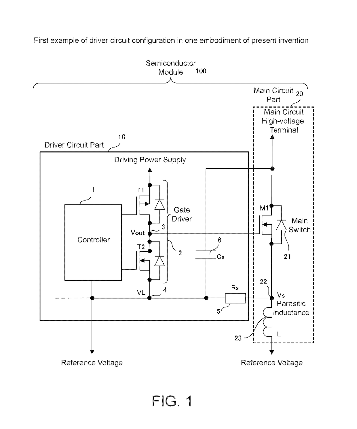
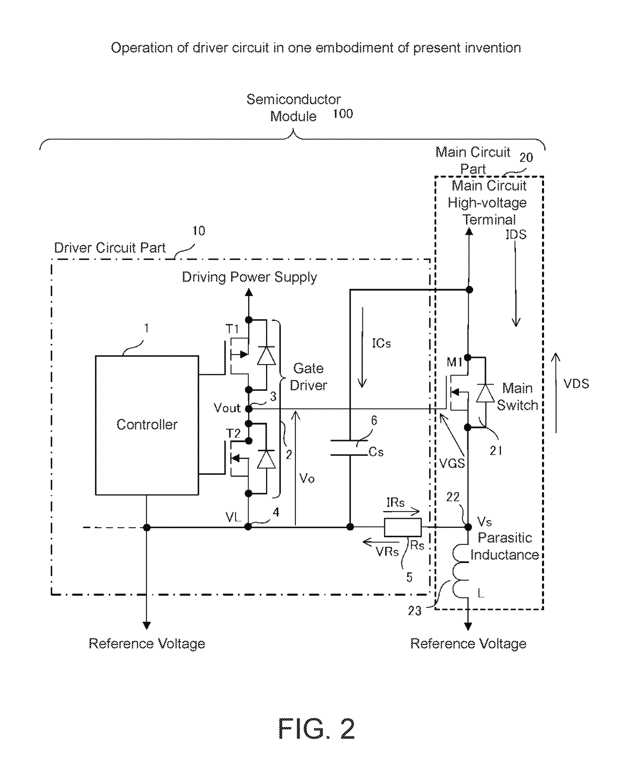
[0037]FIG. 1 illustrates a configuration of a driver circuit according to the embodiment of the present invention. The driver circuit according to the embodiment of the present invention can be generally divided into a driver circuit 10 and a main circuit 20. In this case, the driver circuit 10 and the main circuit 20 can be embedded in a single product to form a semiconductor module 100.

[0038]The driver circuit 10 illustrated in FIG. 1 includes a controller 1 that controls and drives a gate driver 2; the gate driver 2, in which a first transistor T1 and a second transistor T2 are directly connected in series between a driving power supply and a reference voltage, and in which an output (Vout) 3 is obtained from a node between the transistors T1 and T2; a current limiting resistor (RS) 5 connected between a low-voltage side power supply terminal (VL) 4 of the gate driver 2 (the source of the second transi...


PUM


Abstract

An output of a gate driver that drives a main switch is connected to the gate of the main switch, and a low-voltage side power supply terminal of the gate driver is connected to a source of the main switch via a current limiting resistor. Moreover, a suppression capacitor for suppressing rapid changes in current, having a prescribed capacitance, is connected between the drain of the main switch of a main circuit and the low-voltage side power supply terminal of the gate driver. This makes it possible to suppress the rapid change in current that occurs when the main switch switches OFF as well as to prevent extremely large currents from occurring in a low-voltage side power supply line of the driver circuit.

Description

BACKGROUND OF THE INVENTION[0001]Technical Field[0002]The present invention relates to a driver circuit for use in a power converter such as a DC-DC converter or an inverter for driving a motor, and to a semiconductor module including the driver circuit.[0003]Background Art[0004]In discrete power semiconductors such as metal-oxide-semiconductor field-effect transistors (MOSFETs) and insulated-gate bipolar transistors (IGBTs), as well as in intelligent power modules (IPMs) and modules that include such devices in a single product, driver circuits are used to drive the power semiconductor devices (hereinafter, main switches). In the driver circuit illustrated in FIG. 5, for example, an output terminal (Vout) 73 of a gate driver 72 in a driver circuit 70 is connected to the gate of a main switch (M11) 81 of a main circuit 80, another terminal (a low-side power supply terminal (VL) 74 of the driver circuit 70) is connected to a source (VS) 82 of a power semiconductor device (the main sw...

Claims


Application Information

Patent Timeline
Patent Type & Authority Patents(United States)
IPC IPC(8): H03K17/081H02M1/32H02M3/158H03K17/0812H03K17/687H02M1/00
CPCH03K17/08104H02M1/32H02M3/158H03K17/6871H03K17/08122H03K2217/0072H02M2001/0038H03K2217/0063H02M1/0038
Inventor SATO, TADAHIKO
Owner FUJI ELECTRIC CO LTD
Learn More