Forming method of part semiconductor assembly

A technology for semiconductors and components, which is applied in the field of forming some semiconductor components, can solve the problems of inconvenience and lack of suitable manufacturing methods.

Active Publication Date: 2011-02-02
TAIWAN SEMICON MFG CO LTD
View PDF2 Cites 0 Cited by
  • Summary
  • Abstract
  • Description
  • Claims
  • Application Information

AI Technical Summary

Problems solved by technology

[0005] It can be seen that the above-mentioned existing method for forming semiconductor components obviously still has inconvenience and defects in the manufacturing method and use, and needs to be further improved urgently.
In order to solve the problems existing in the formation methods of some semiconductor components, the relevant manufacturers have tried their best to find a solution, but for a long time no suitable design has been developed, and the general manufacturing method has no suitable manufacturing method to solve it. The above-mentioned problems are obviously the problems that relevant industry players are eager to solve

Method used


Image

  • Forming method of part semiconductor assembly
  • Forming method of part semiconductor assembly
  • Forming method of part semiconductor assembly

Examples


Embodiment Construction

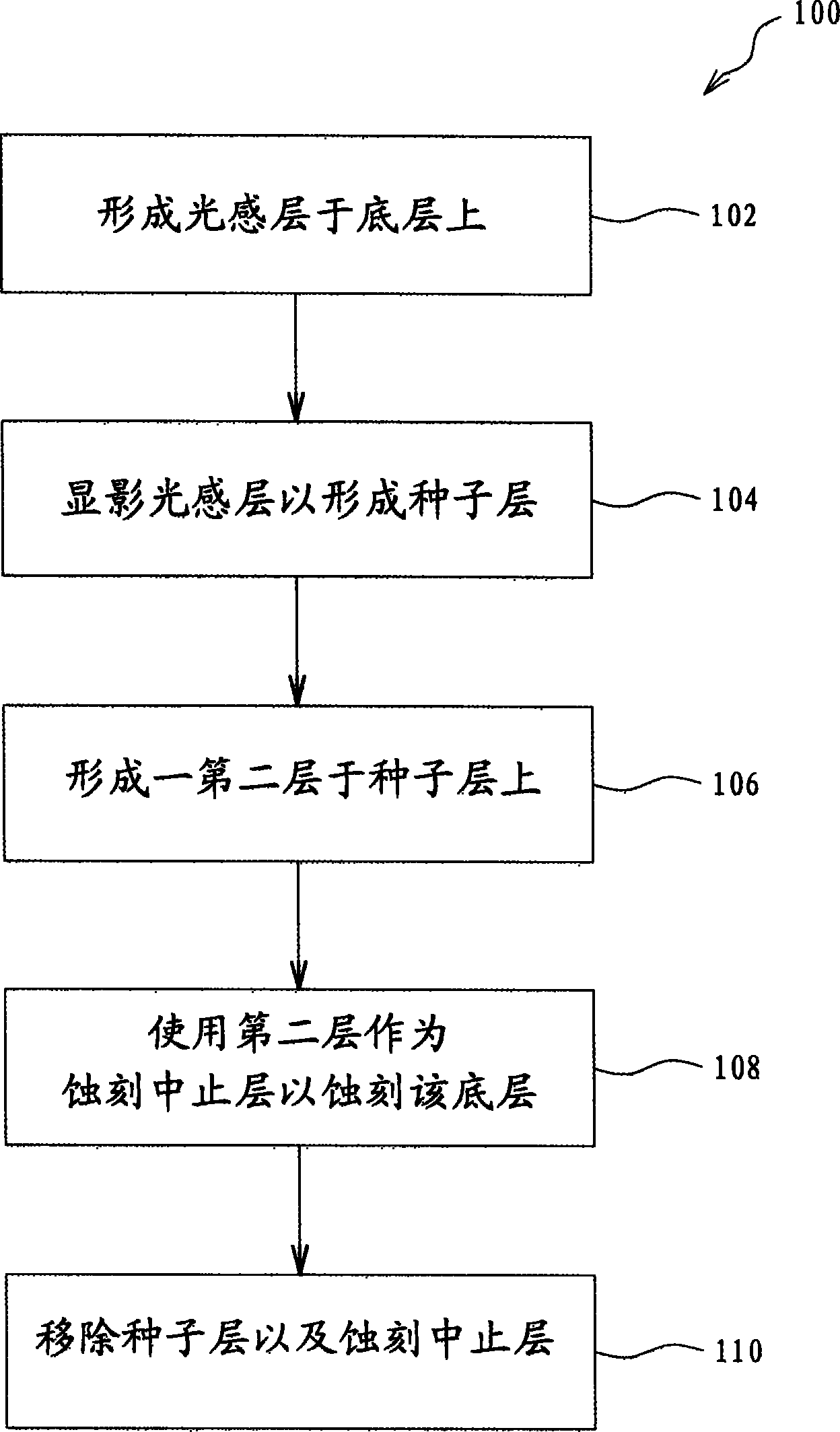
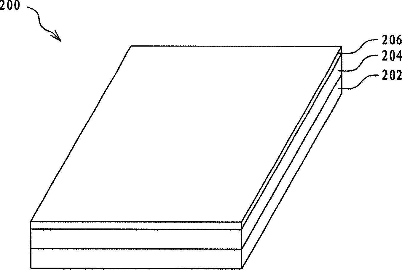
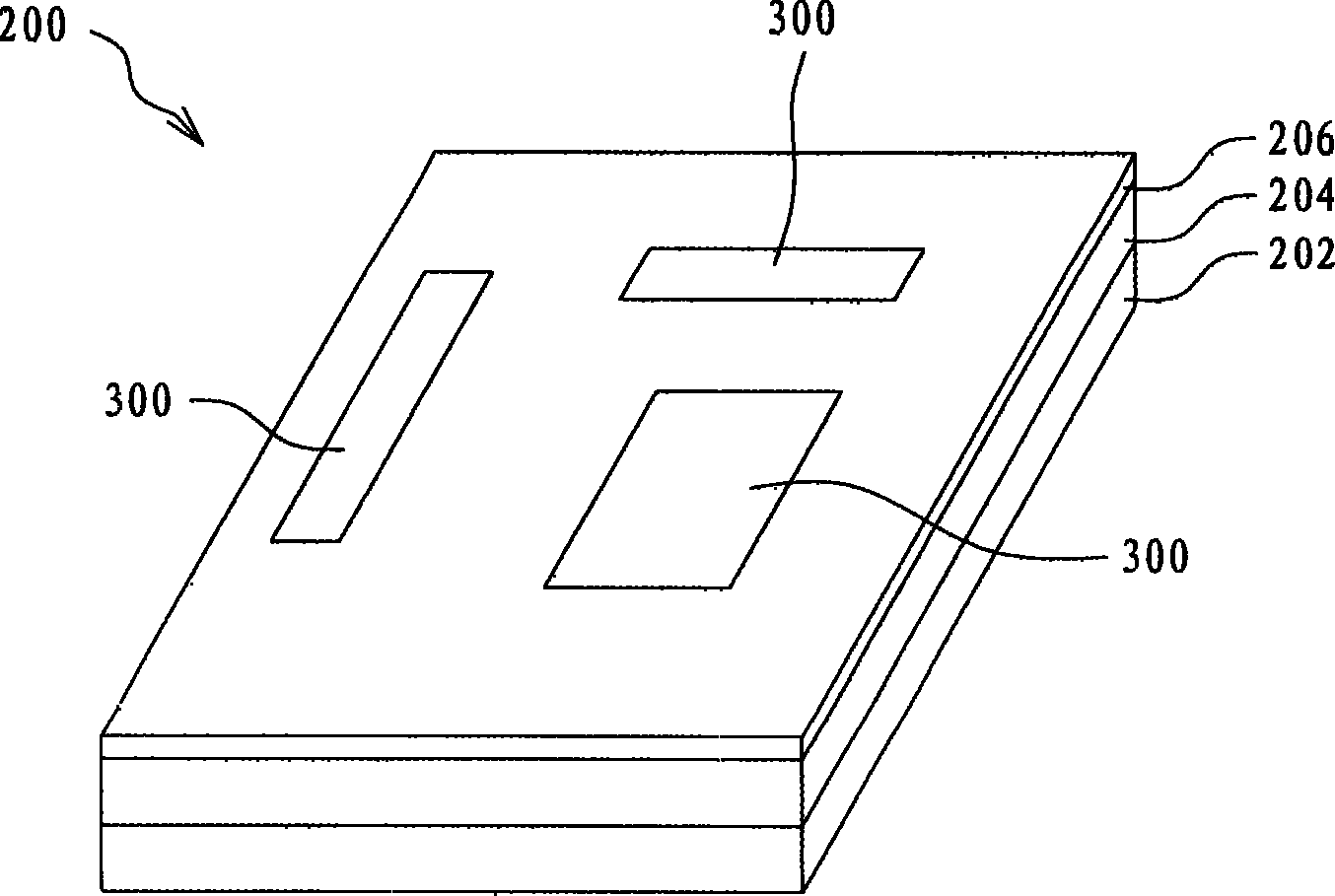
[0058] In order to further illustrate the technical means and effects that the present invention adopts for reaching the intended purpose of the invention, below in conjunction with the accompanying drawings and preferred embodiments, its specific implementation, method (manufacturing method) of the method for forming part of the semiconductor component proposed according to the present invention , processing method), steps, features and effects thereof, detailed descriptions are as follows.

[0059] The invention to be disclosed next provides many different embodiments, or examples, to illustrate different features of the invention. The following specific examples of constituent elements and arrangements will facilitate understanding of the present invention. Of course, these examples are not intended to limit the present invention. In addition, some reference numerals or nouns are repeated in various embodiments of the present invention, which is for the purpose of simplify...


PUM


Abstract

The present disclosure relates generally to the manufacturing of semiconductor devices. In one example, a method for forming a portion of a semiconductor device includes forming a photo sensitive layer over a substrate, developing the photo sensitive layer to expose a portion of the substrate and to create a seed layer from at least a portion of the photo sensitive layer remaining after the developing, forming an etch stop layer only on the seed layer, and etching the substrate using the etch stop layer as a mask.

Description

technical field [0001] The invention relates to a method for forming a part of a semiconductor component, in particular to a method for forming a part of a semiconductor component using a photolithography process. Background technique [0002] The margin of the depth of focus is a factor in the semiconductor device manufacturing process. In general, an effective depth of focus is fully applicable to variations in photoresist thickness, such as local substrate topology step heights and height differences between the center and edge of the wafer. Using an effective depth of focus can make it easier for the semiconductor device to be manufactured within critical dimensions, and the semiconductor device has little or no scum or toploss defects. [0003] Problems can occur where the photoresist is thicker than the depth of focus. For example, if the depth of focus is less than the combined thickness of the photoresist layer and the step height variation, scum or CD errors may o...

Claims


Application Information

Patent Timeline
Patent Type & Authority Patents(China)
IPC IPC(8): H01L21/308G03F7/00H01L21/027
CPCG03F7/405G03F7/40H01L21/31144H01L21/0271H01L21/32139H01L21/0332H01L21/0274
Inventor 林进祥
Owner TAIWAN SEMICON MFG CO LTD
Why Eureka
Try Eureka