Field emission element in use for background light

A technology of emitting elements and field emission, which is applied in optics, instruments, nonlinear optics, etc., can solve the problems of high power consumption, energy reduction, and efficiency reduction, and achieve the goal of reducing power consumption, reducing possibility, and ensuring stability Effect

Inactive Publication Date: 2007-05-09
LG ELECTRONICS(NANJING) PLASMA CO LTD
View PDF0 Cites 4 Cited by
  • Summary
  • Abstract
  • Description
  • Claims
  • Application Information

AI Technical Summary

Problems solved by technology

At the same time, because the field emission element is a vacuum element, spacers are used in order to support the upper substrate and the lower substrate. Since the spacers must not be exposed in front of the screen, in order to fully ensure the distance between the upper and lower plates, the spacer must be made The shape of the column is higher than the contact part of the upper and lower plates, so there are difficulties in manufacturing
That is, if the anode voltage is set, phenomena such as an arc generated by a high voltage will occur, and the stability of the element will be reduced, so it will be difficult to increase the voltage
[0013] Second, if the anode voltage is set to increase the discharge current, as the discharge current increases, the current density is also increased, and as the current density increases, the efficiency will decrease.
That is, as shown in FIG. 2, if the screen voltage increases from V1 to V2, the concentration of the electron beams emitted by the carbon nanotubes 31 formed on the lower substrate 30 increases from D1 to D2, and the electron beams and the upper substrate 33 The part where the fluorescent body 32 collides is different, so the deviation of the current density will occur
[0014] Third, similar to the CRT phosphor, if an Al white layer (not shown in the figure) is formed, the efficiency increases, but when the electrons emitted by the bottom voltage collide with the Al white layer, the energy of the emitted electrons decreases. Therefore, there will be a problem that the phosphor cannot be sufficiently irradiated.
At the same time, although the gray scale of the electron beams emitted by the carbon nanotubes is increased, the efficiency is reduced. Although the efficiency of the electron beams is not concentrated, although the efficiency of the electron beams is high, the electron beams for producing gray scales cannot sufficiently cause collisions, so the overall Generally speaking, it will cause a large power consumption

Method used


Image

  • Field emission element in use for background light
  • Field emission element in use for background light
  • Field emission element in use for background light

Examples


Embodiment Construction

[0032] Below, the preferred embodiment of the field emission element for the backlight according to the present invention will be referred to the accompanying drawings.

[0033] Examples are described in detail.

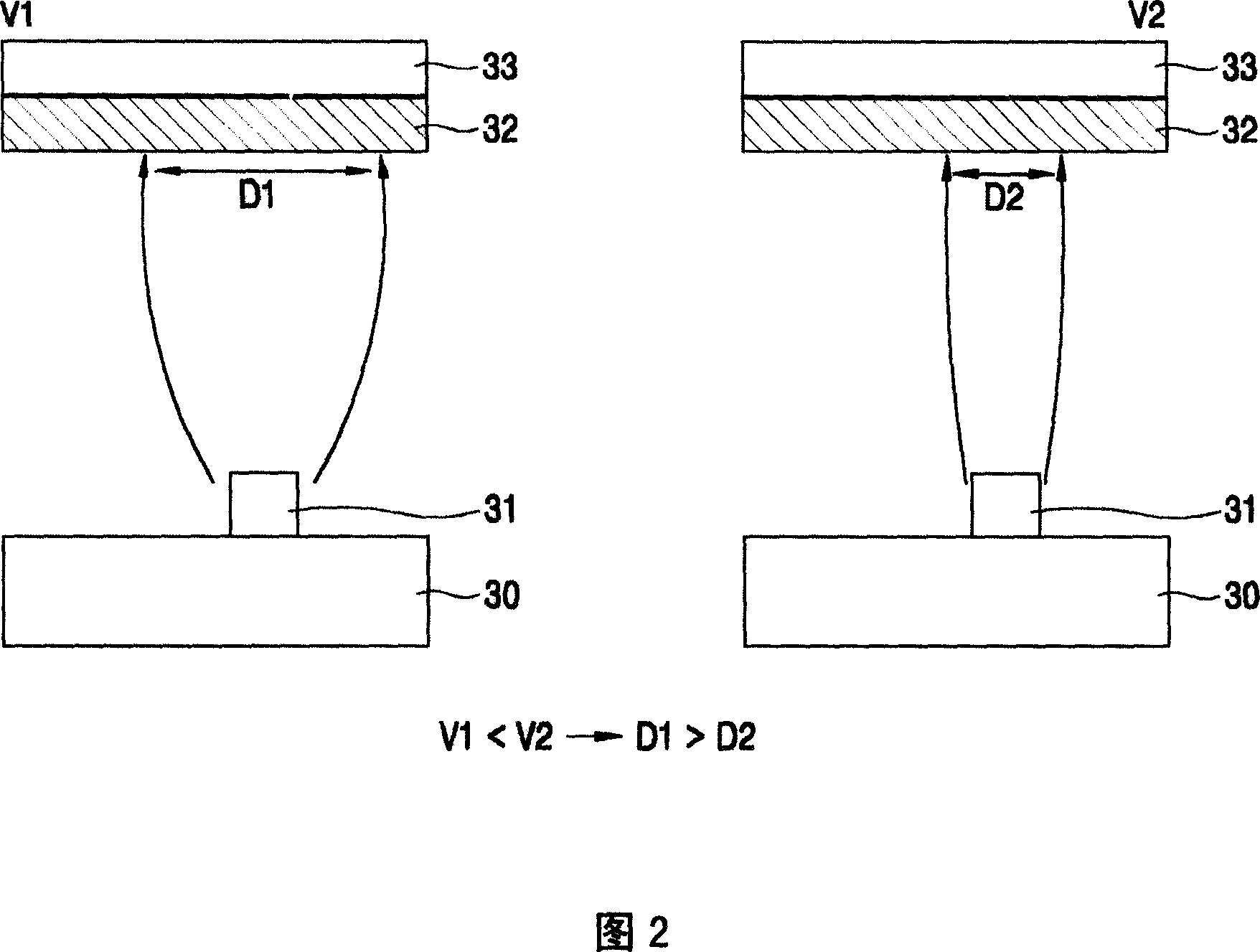
[0034] Generally speaking, the efficiency of the backlight is expressed by "efficiency=brightness×π×display area / power". It can be known from the formula that efficiency is directly proportional to brightness and display area, and inversely proportional to power.

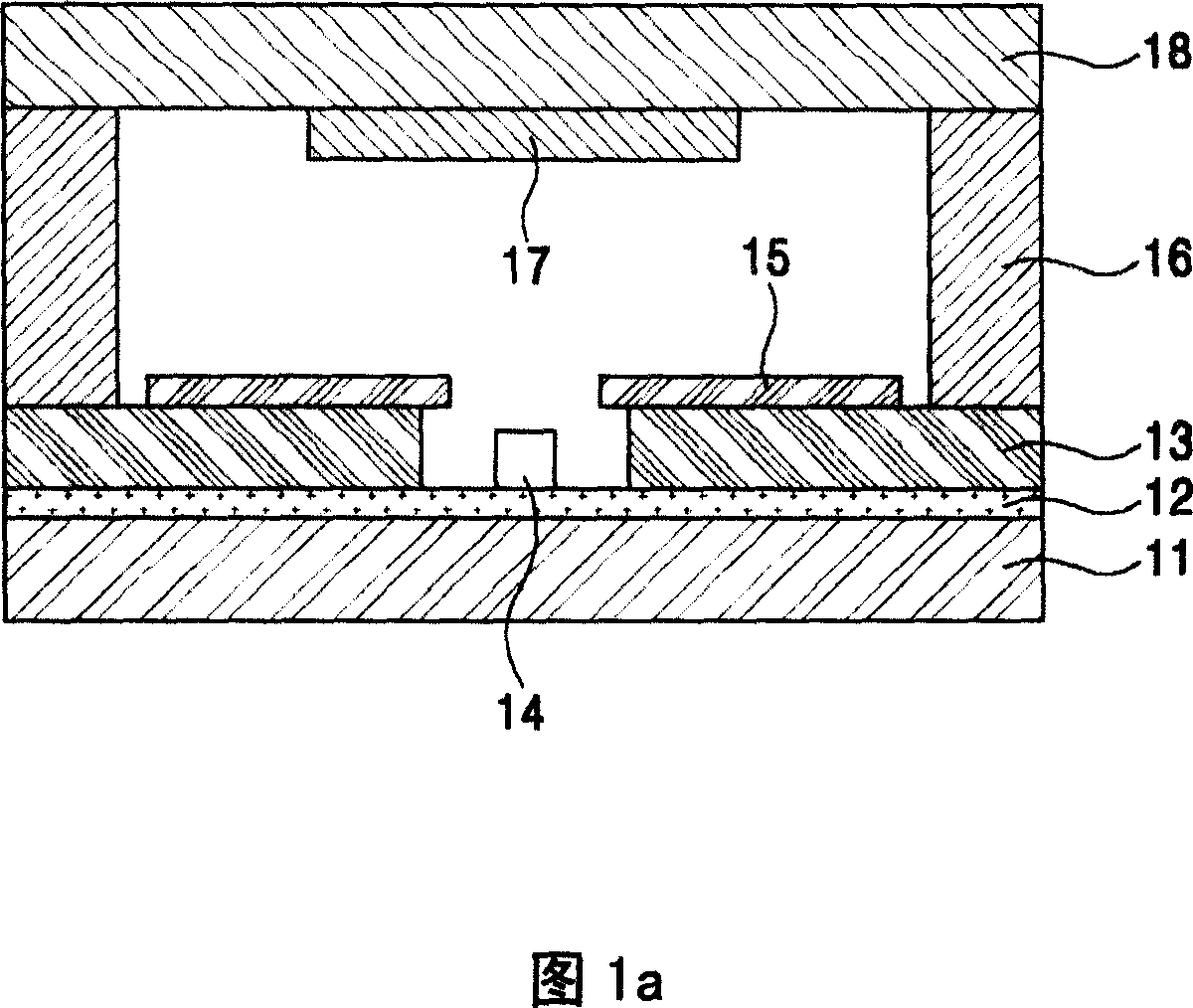
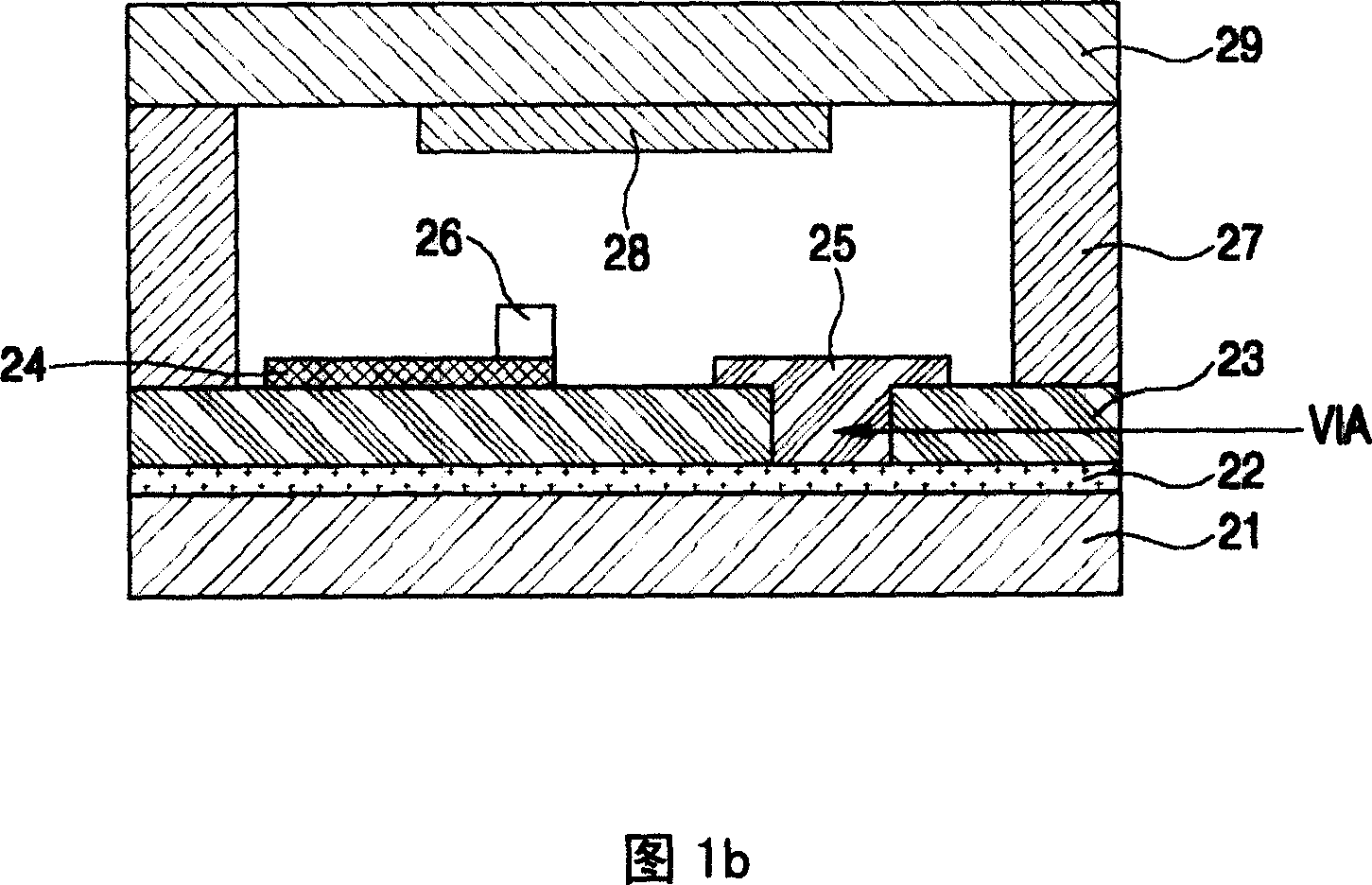
[0035] The main features of the present invention are as follows: the shape of the fluorescent surface that collides with the electrons released from the carbon nanotube to emit light is a protruding surface structure, and the surface area of ​​the fluorescent body that collides with the emitted electrons is enlarged.

[0036] Fig. 3 shows a cross-sectional view of a carbon nanotube field emission element with a counter electrode bottom gate structure for a background light according to the present invent...


PUM


Abstract

A field emission element used on background lamp makes form of fluorescent surface on fluorescent body be a projected surface in order to increase coating area of fluorescent body for raising efficiency of field emission element utilizing carbon nanotube as electronic emission source.

Description

technical field [0001] The present invention relates to a field emission element for a background light, in particular to an application for a background light in which the shape of the fluorescent surface of the fluorescent body formed by the field emission element using carbon nanotubes as an electron emission source is a protruding surface, thereby increasing the coating area of ​​the fluorescent body to the emitting element. Background technique [0002] Recently, as various display devices are developed, the importance of light sources is also being increased. These light sources use various methods such as heating a filament, using gas discharge, and emitting light from a phosphor. These light sources can only be used as simple lighting equipment, but they can also be used as display backlights such as LCDs in the form of surface light sources. [0003] The backlight of this kind of LCD mainly uses a fluorescent lamp (Flourescent Lamp: FL) that can improve a very hig...

Claims


Application Information

Patent Timeline
IPC IPC(8): G02F1/13357H01J1/30G02F1/1335
Inventor 权奇振
Owner LG ELECTRONICS(NANJING) PLASMA CO LTD
Why Eureka
Try Eureka