
Shared voltage modification circuit and method

A common voltage and circuit correction technology, which is applied to instruments, static indicators, etc., can solve problems such as poor display quality and wrong gray-scale voltage of thin-film transistors, so as to save the number of process masks, ensure picture quality, and correct gray-scale voltage Effect

Inactive Publication Date: 2007-04-04
CHUNGHWA PICTURE TUBES LTD
View PDF1 Cites 9 Cited by
  • Summary
  • Abstract
  • Description
  • Claims
  • Application Information

AI Technical Summary

Problems solved by technology

If the above-mentioned invention of US Pat. No. 6,392,623 is applied to a thin-film transistor liquid crystal display panel (thin-film transistor liquid crystal display panel) using an AC common voltage, it will cause grayscale voltage errors when the thin-film transistor is turned off, resulting in poor display quality.

Method used


Image

  • Shared voltage modification circuit and method
  • Shared voltage modification circuit and method
  • Shared voltage modification circuit and method

Examples


Embodiment Construction

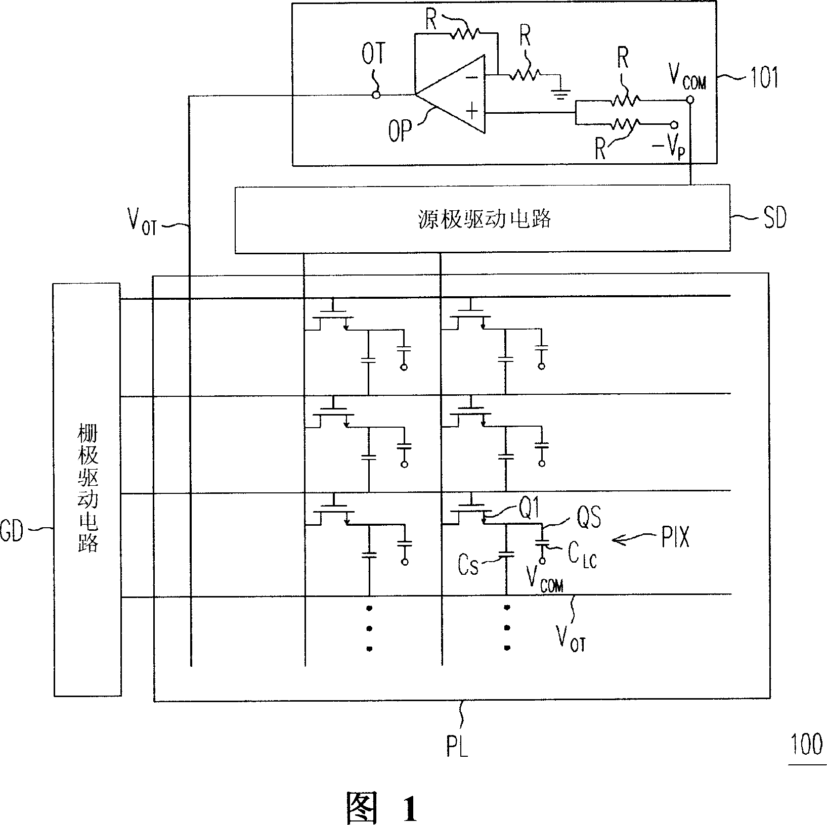
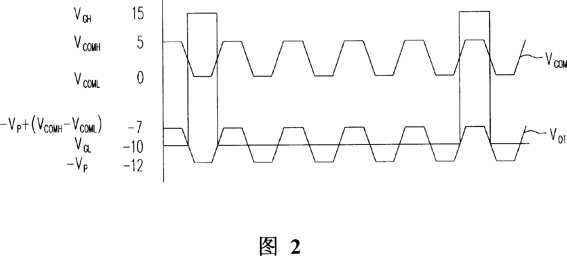
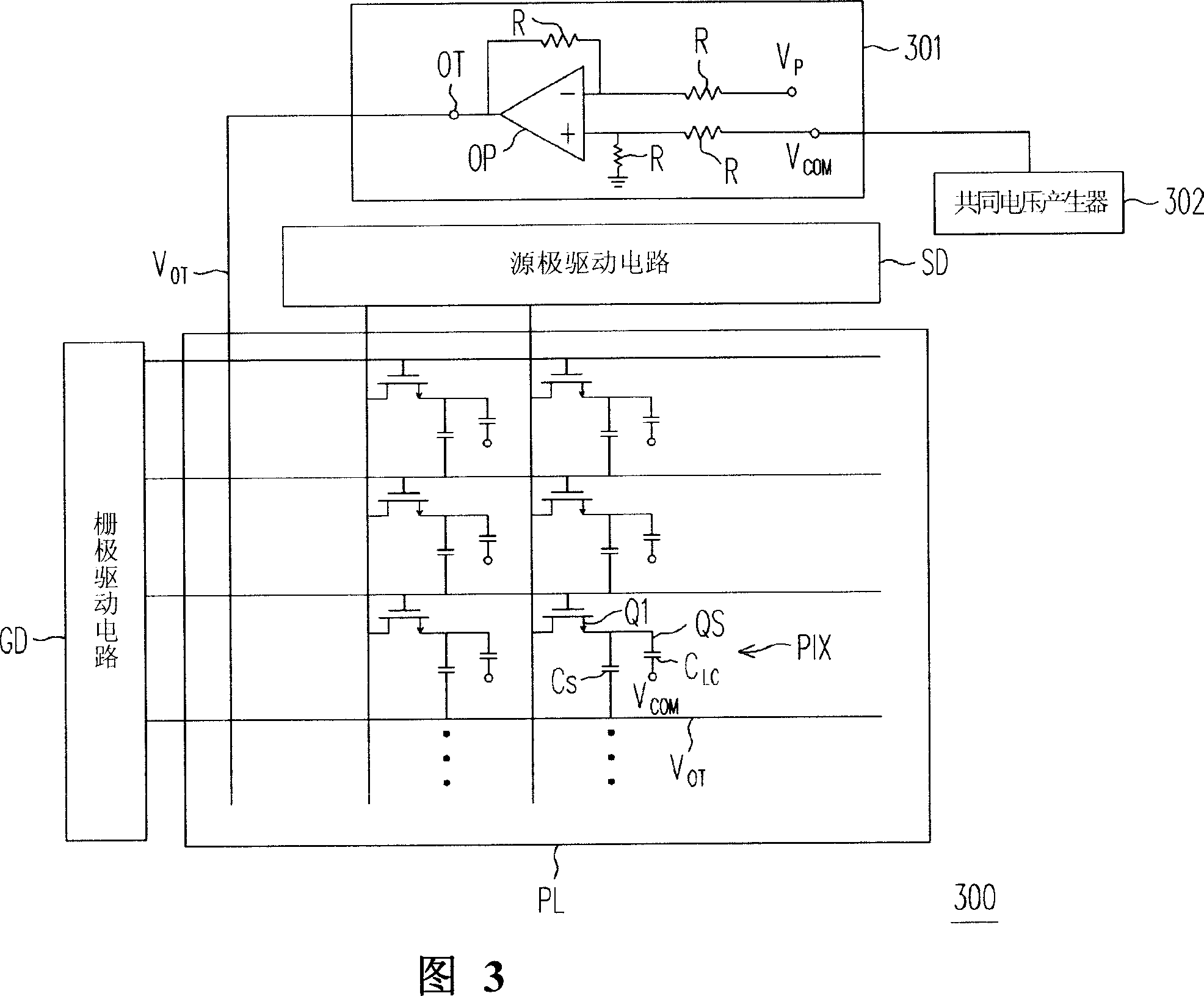
[0039] Please refer to FIG. 1 for the following description. FIG. 1 is a partial circuit diagram of a thin film liquid crystal display 100 according to a first embodiment of the present invention. The circuit in FIG. 1 includes a source driver circuit SD, a gate driver integrated circuit GD, a thin film liquid crystal display panel PL, and an arithmetic circuit 101 . The common voltage correction circuit of this embodiment includes an arithmetic circuit 101 and a source driver circuit SD.

[0040] Although the thin film liquid crystal display panel PL of FIG. 1 shows only 6 pixels, any number of pixels may actually be included. For example, the enlarged pixel PIX in FIG. 1 includes a thin film transistor Q1 , a storage capacitor Cs, and a liquid crystal capacitor CLC. The gate of the thin film transistor Q1 is electrically connected to the gate driving circuit GD, and the drain is electrically connected to the source driving circuit SD. One end of the storage capacitor Cs is...


PUM


Abstract

This invention is a coordinating voltage corrector circuit and its working method. Coordinating voltage allows AC modulation and reduces power consumption. By use of metal insulation semi-conductor capacitance could reduce the cost and guarantee the accuracy of gray scale voltage. The character of this invention is that the capacitance is capable of outputting voltage to each pixel on film LCD according to pre-set and coordinating voltage. The output voltage and coordinating voltage are all AC voltage. Each LCD capacitance is linked to coordinating voltage. Output voltage and coordinating voltage are of the same phase and swing. The pre-set voltage value is equal to the difference of coordinating voltage and output voltage.

Description

technical field [0001] The present invention relates to a common voltage (common voltage) correction circuit and method for a thin-film transistor liquid crystal display (referred to as TFT LCD), and in particular to a method for correcting alternating current (referred to as TFT LCD). A common voltage correction circuit and method for AC) modulation. Background technique [0002] A pixel of a general thin film liquid crystal display includes a thin film transistor, a storage capacitor, and a liquid crystal capacitor. If a metal-insulator semiconductor (MIS for short) structure is used as the storage capacitor, the number of process masks can be reduced and the manufacturing cost can be reduced. [0003] U.S. Patent No. US 6392623 proposes that in the structure of the storage capacitor formed by the metal insulating layer semiconductor, different electrodes are applied to the common electrode connected to one end of the storage capacitor and the counter electrode connected ...

Claims


Application Information

Patent Timeline
Patent Type & Authority Applications(China)
IPC IPC(8): G09G3/36G09G3/20G02F1/133
Inventor 陈昱丞施奕丞林代明
Owner CHUNGHWA PICTURE TUBES LTD
Learn More