Wafer grinding and cutting process

A cutting method and wafer technology, applied in electrical components, semiconductor/solid-state device manufacturing, circuits, etc., can solve the problems of chipping before cutting, wafer scratches, wafer exposure, etc., to reduce scratches, The effect of avoiding scratches and improving the yield

Inactive Publication Date: 2007-03-21
NANTONG FUJITSU MICROELECTRONICS
View PDF0 Cites 2 Cited by
  • Summary
  • Abstract
  • Description
  • Claims
  • Application Information

AI Technical Summary

Problems solved by technology

[0003] The present invention aims to solve the technical problem that the wafer is exposed after grinding in the conventional IC packaging common wafer grinding and cutting process, and foreign objects are easy to touch the wafer, causing scratches, fragmentation, and crushing of the chip before cutting, and provides a Wafer grinding and cutting method capable of solving the above-mentioned technical problems

Method used


Image

  • Wafer grinding and cutting process
  • Wafer grinding and cutting process

Examples


Embodiment Construction

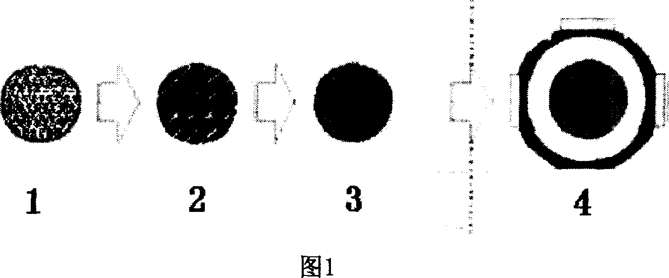
[0010] In the present invention, the existing normal ordinary wafer grinding and cutting process sequence is adjusted from 1-2-3 (①wafer film before grinding; Wafer film (3) before cutting (2) peeling after operation) to reduce chip scratches, crushing and chipping.

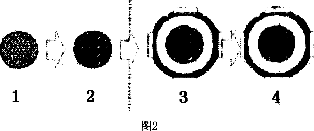
[0011] Therefore, concrete method steps of the present invention: (as shown in Figure 2)

[0012] 1. Before grinding, the wafer is first coated with a film and then ground;

[0013] 2. Paste the wafer on the bracket with adhesive tape before cutting the disc after grinding;

[0014] 3. After the wafer is pasted, the film is peeled off;

[0015] 4. The wafer after peeling off the film can be operated on the cutting machine.


PUM


Abstract

The wafer grinding and cutting process includes the specific steps: adhering film to be ground, adhering wafer to be cut, uncovering the film after adhering wafer and operating the wafer in the cutter. The present invention recovers the film before cutting, rather than after the grinding operation, and this can avoid the exposure of the ground wafer, avoid scoring and fragmentation effectively and raise the finished product rate of wafer grinding and cutting operation.

Description

technical field [0001] The invention relates to an IC packaging process method, in particular to a process method for effectively preventing scratches and crushing on the surface of a wafer and improving the yield rate of the wafer after it is broken. Background technique [0002] At present, the known common wafer grinding and cutting process for IC packaging (as shown in Figure 1) is: 1. Wafer film application before grinding, 2. Film removal after operation, 3. Chip placement before cutting, 4. Wafer placement after cutting on the stand. During the period, the opportunity for the wafer to be exposed in the space appears after the grinding operation, which increases the number of foreign objects touching the wafer, causing scratches, fragmentation, and crushing of the wafer before cutting. The placement of the broken wafer will not be possible. Chip position identification cannot be performed on wafers of chips. Contents of the invention [0003] The present invention ...

Claims


Application Information

Patent Timeline
Patent Type & Authority Applications(China)
IPC IPC(8): B24B1/00H01L21/304
Inventor 许海渐
Owner NANTONG FUJITSU MICROELECTRONICS
Why Eureka
Try Eureka