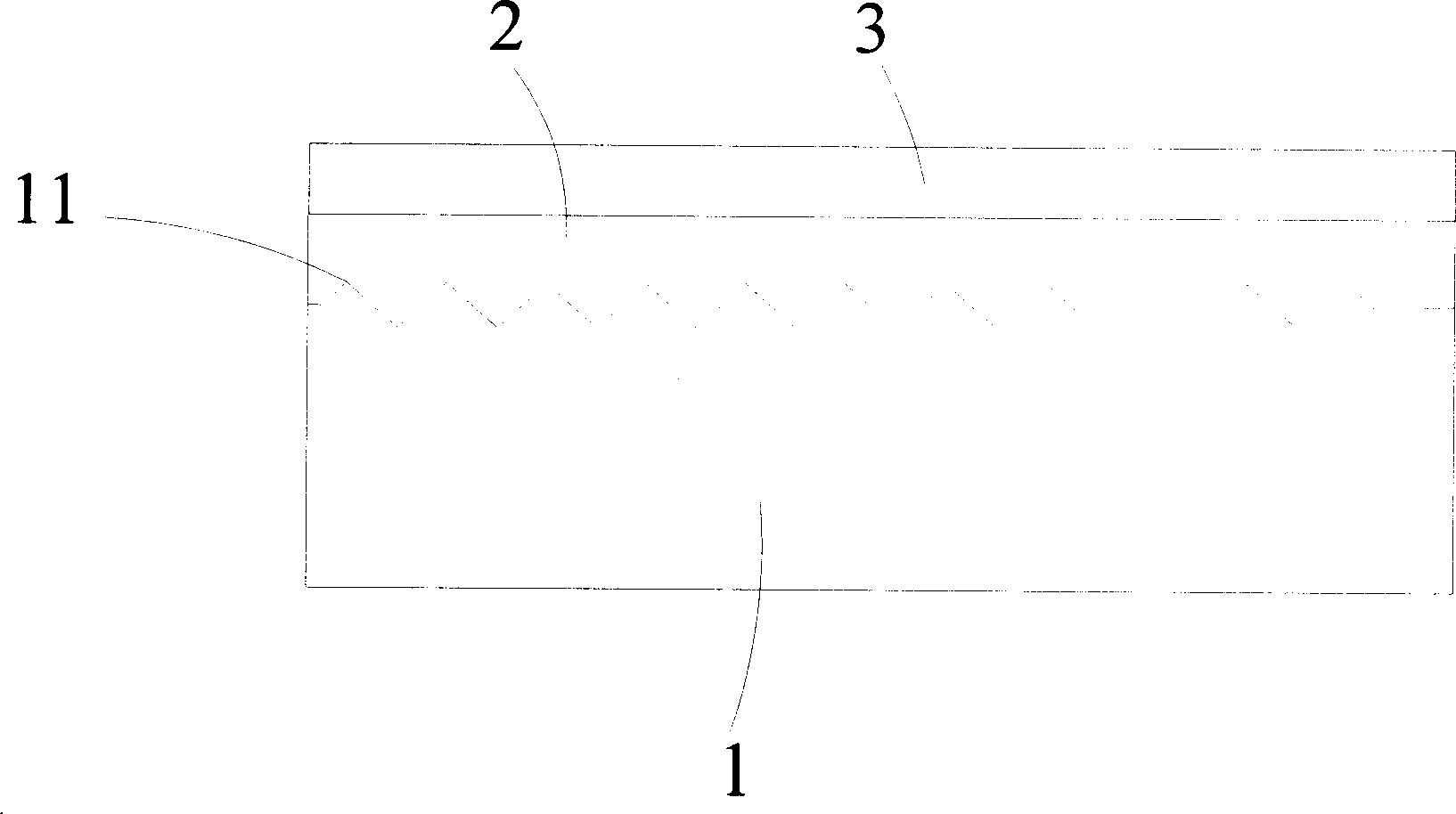
LCP substrate sputtering coating treatment against EMI coating
A substrate and sputtering technology, which is applied in the field of coating pretreatment in the sputtering method, can solve the problems of reducing the adhesion between the substrate and the film layer, long current pulse path, poor anti-EMI effect, etc., and achieve enhanced anti-EMI effect , reduce the unit impedance, enhance the effect of adhesion
- Summary
- Abstract
- Description
- Claims
- Application Information
AI Technical Summary
Problems solved by technology
Method used
Image
Examples
Embodiment 1
[0030] A method for coating a LCP base material, comprising the steps of:
[0031] Sand blasting treatment step, under the air pressure of 0.02MPa, carry out sand blasting treatment to the substrate surface with 180# white corundum sand grains;
[0032] In the cleaning step, the surface of the substrate that has been sandblasted is cleaned with ultrasonic waves, and the sand particles on the surface of the substrate are washed away;
[0033] In the primer coating step, a layer of primer is sprayed on the surface of the cleaned substrate. The primer can be glossy or matte, and the thickness is controlled at 5 μm, and then cured by UV;
[0034] For the coating, a copper film with a thickness of about 0.5 μm is plated on the surface by vacuum sputtering physical coating method.
Embodiment 2
[0036] A method for coating a LCP base material, comprising the steps of:
[0037] Sand blasting treatment step, under the air pressure of 0.05MPa, carry out sand blasting treatment to the substrate surface with 180# brown corundum sand grains;
[0038] In the cleaning step, the surface of the substrate that has been sandblasted is cleaned with ultrasonic waves, and the sand particles on the surface of the substrate are washed away;
[0039] In the primer coating step, a layer of primer is applied on the surface of the cleaned substrate by dip coating. The primer can be glossy or matte, and the thickness is controlled at 20 μm, and then cured by UV;
[0040] For the coating, a copper film with a thickness of about 0.5 μm is plated on the surface by vacuum sputtering physical coating method.
PUM
| Property | Measurement | Unit |
|---|---|---|
| thickness | aaaaa | aaaaa |
Abstract
Description
Claims
Application Information
 - R&D
- Intellectual Property
- Life Sciences
- Materials
- Tech Scout
- Unparalleled Data Quality
- Higher Quality Content
- 60% Fewer Hallucinations
Browse by: Latest US Patents, China's latest patents, Technical Efficacy Thesaurus, Application Domain, Technology Topic, Popular Technical Reports.
© 2025 PatSnap. All rights reserved.Legal|Privacy policy|Modern Slavery Act Transparency Statement|Sitemap|About US| Contact US: help@patsnap.com

