
Driving circuit for organic light emitting diode, display device using the same

一种发光二极管、驱动电路的技术,应用在静态指示器、电致发光光源、仪器等方向,能够解决OLED驱动电路15可靠性劣化、OLED显示器可靠性劣化等问题

Active Publication Date: 2006-12-27
LG DISPLAY CO LTD
View PDF0 Cites 11 Cited by
  • Summary
  • Abstract
  • Description
  • Claims
  • Application Information

AI Technical Summary

Problems solved by technology

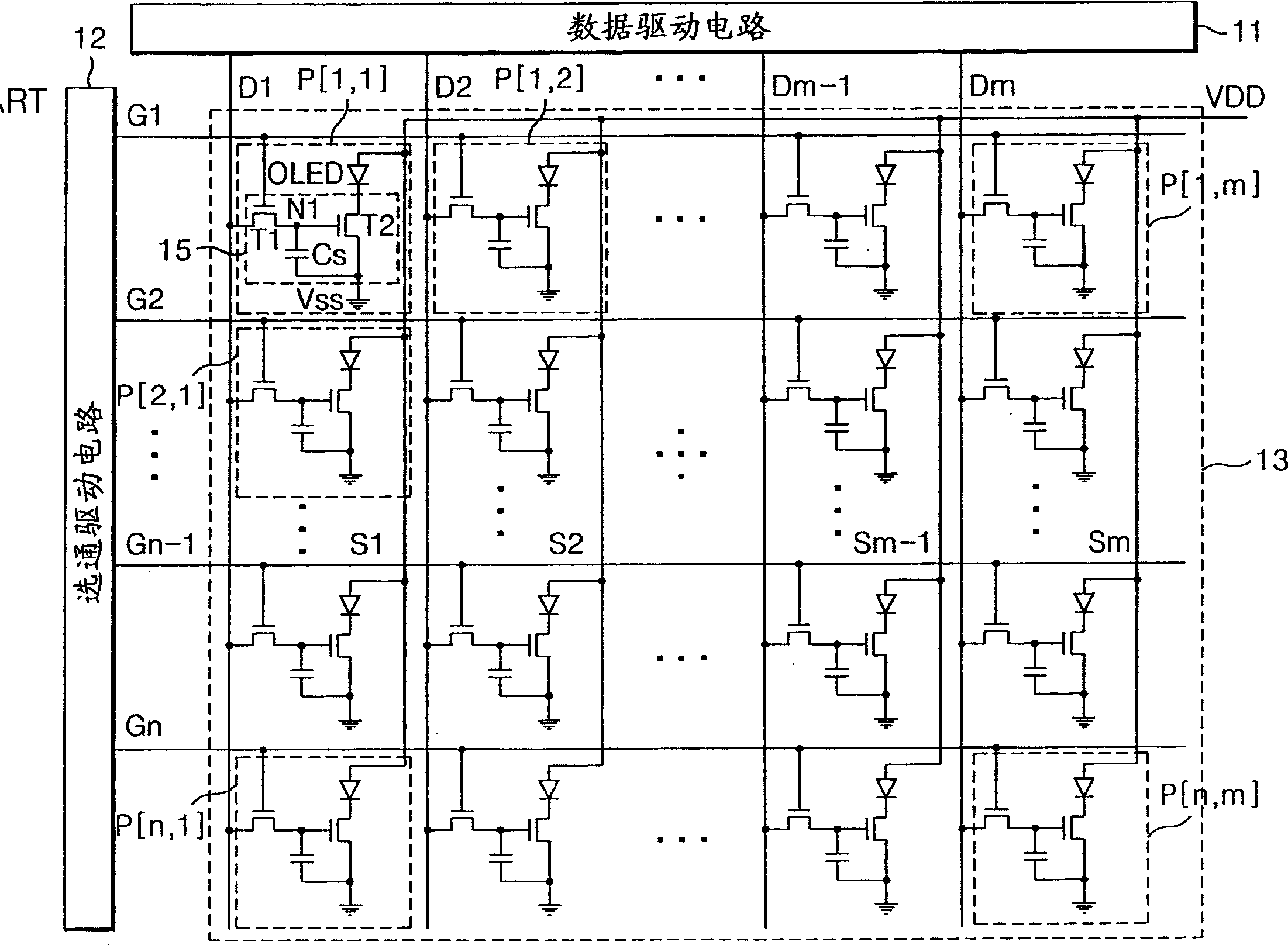
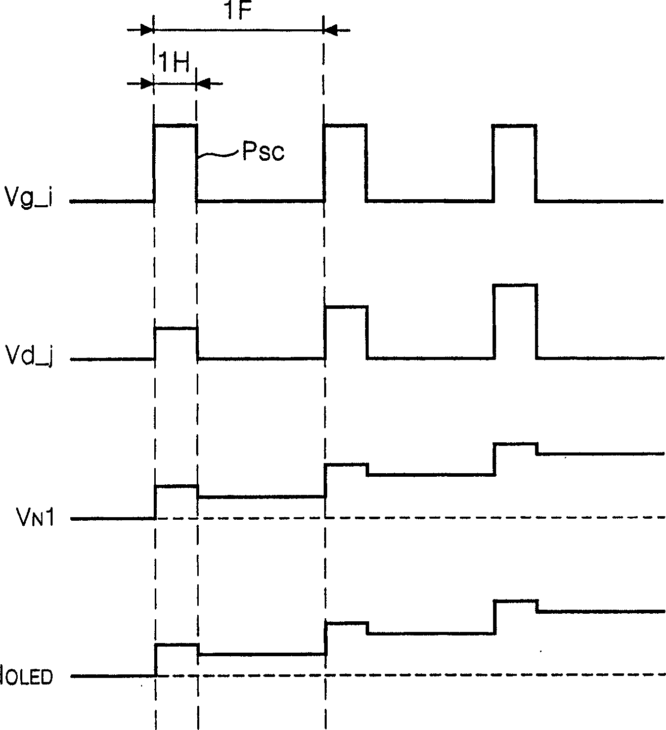
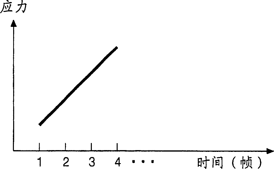
In this way, the characteristic variation of the OLED driving device such as the second transistor T2 generated by the gate bias stress changes the current flowing into the OLED, deteriorating the reliability of the operation of the OLED driving circuit 15, and further making the reliability of the operation of the OLED display Sexual deterioration

Method used


Image

  • Driving circuit for organic light emitting diode, display device using the same
  • Driving circuit for organic light emitting diode, display device using the same
  • Driving circuit for organic light emitting diode, display device using the same

Examples


Embodiment Construction

[0045] Reference will now be made in detail to the preferred embodiments of the invention, examples of which are illustrated in the accompanying drawings.

[0046] The following will refer to Figures 5 to 9 Embodiments of the present invention are explained.

[0047] refer to Figure 5 , the OLED display according to the present invention includes: an OLED panel 103 having a region defined by the intersection of n gate lines G1 to Gn (n is a positive integer) and m data lines D1 to Dm (m is a positive integer) n×m pixels P[i,j] arranged in an n×m matrix shape in (P[i,j] is a pixel located at row i and column j, i is a positive integer equal to or less than n, and j is a positive integer equal to or less than m); a gate drive circuit 102, which drives the gate lines G1 to Gn of the OLED panel 103; a data drive circuit 101, which drives the data lines D1 to Dn of the OLED panel 103; m power supplies voltage supply lines S1 to Sm arranged in parallel with the data lines D1 to ...


PUM


Abstract

The invention relates to an organic light emitting diode driving circuit adaptive for preventing organic light emitting diode driving equipment characteristic changes and an organic light emitting diode display employing the drive circuit. The organic light emitting diode drive circuit includes an organic light emitting diode which emits light with a current, a first transistor, a second transistor and a stress compensation circuit. The first transistor supplies a data voltage to a first node in response to a scan pulse. The second transistor controls a current flowing in the organic light emitting diode by the data voltage on the first node. The stress compensation circuit discharges the first node in response to a reset pulse. The organic light emitting diode driving circuit is adaptive to compensate characteristic changes of the organic light emitting diode drive circuit.

Description

technical field [0001] The present invention relates to an organic light emitting diode display, and more particularly, to an organic light emitting diode driving circuit suitable for preventing variations in characteristics of an organic light emitting diode driving device, and an organic light emitting diode display using the driving circuit. Background technique [0002] Recently, various flat panel displays capable of reducing their weight and size, which are disadvantages of cathode ray tubes CRTs, have appeared. The flat panel display includes a liquid crystal display LCD, a field emission display FED, a plasma display panel PDP, a light emitting diode (hereinafter referred to as "LED") display, and the like. [0003] Among these displays, LED displays use LEDs that make phosphors emit light by recombining electrons and holes. LED displays are classified into inorganic light emitting diode LED displays using inorganic compounds as phosphors and organic light emitting ...

Claims


Application Information

Patent Timeline
Patent Type & Authority Applications(China)
IPC IPC(8): G09G3/32G09G3/30H05B33/08H05B33/14H05B44/00
CPCG09G3/3291G09G2320/043G09G2300/043G09G3/3233G09G2300/0847G09G2310/0254G09G3/30
Inventor 尹洙荣全敏斗
Owner LG DISPLAY CO LTD
Learn More