Stack architecture of multiple chips

A stack structure, multi-chip technology, applied in the direction of electrical components, electrical solid devices, circuits, etc., can solve the problems of increasing the projected area, violating the requirements of small size and multi-functional characteristics of electronic products, affecting the area of ​​electronic products, etc. Number, effect of promoting convenience

Active Publication Date: 2006-12-06
SILICONWARE PRECISION IND CO LTD
View PDF1 Cites 2 Cited by
  • Summary
  • Abstract
  • Description
  • Claims
  • Application Information

AI Technical Summary

Problems solved by technology

[0005] Although the above-mentioned existing multi-chip stacking structure saves space compared with the side-by-side chip method, and can stack the chips first and then perform the wire bonding operation, its biggest disadvantage is that when stacking more layers of chips, the stacking method makes it constantly tilt to one side , so that the projected area of ​​the entire chip stack is bound to increase continuously, such as Figure 1B As shown, assuming that the side length of the semiconductor chip is S, each additional stacked semiconductor chip must be far away from the pad area L of the lower semiconductor chip, so as to facilitate...

Method used


Image

  • Stack architecture of multiple chips
  • Stack architecture of multiple chips
  • Stack architecture of multiple chips

Examples


Embodiment

[0019] The implementation of the present invention will be described below through specific specific examples. The following drawings only show the components related to the present invention, and are not drawn according to the number, shape and size of the components in actual implementation. More complex.

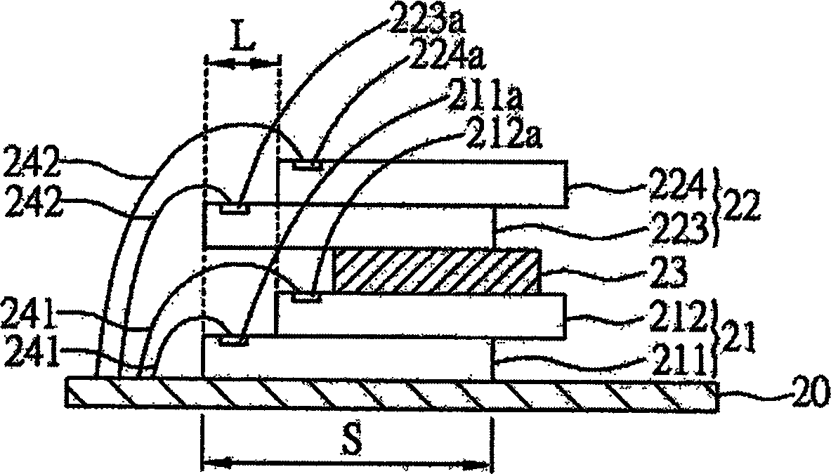
[0020] figure 2 It is a schematic cross-sectional view of the multi-chip stack structure of the present invention.

[0021] The multi-chip stack structure includes: a chip carrier 20 , a first chip set 21 , a buffer 23 and a second chip set 22 . Wherein, the first chipset 21 has a plurality of chips, and these chips have single side pads and are stacked on the chip carrier 20 in a ladder shape, and the pads are exposed; the buffer member 23 is connected to the first chip on the group 21; the second chip group 22 has a plurality of chips, these chips have single-side pads and are stacked on the buffer member 23 in a ladder shape, and the bottom chip of the second chip ...


PUM


Abstract

The stack frame of multiple chips includes carrier for chips, first chipset, cushion piece, and second chipset. The first chipset possesses multiple chips. Possessing unilateral weld pads, these chips are stacked on carrier for chips in stair shape. The cushion piece is joined to the first chipset. Possessing unilateral weld pads, the first chipset possesses multiple chips. Bottommost chip in the second chipset is joined to the cushion piece in deflection towards direction of weld pads of the first chipset. Then, the second chipset is stacked on carrier in stair shape. Weld pads are revealable in order to prevent stack of chips from exceeding packaging region. The invention encapsulates chips in multiple layers to package without increasing area of package. Being able to be stacked in package, multiple chips does not deviate stack in single direction so as to facilitate throwing for weld part of chip.

Description

technical field [0001] The invention relates to a multi-chip stacking structure, in particular to a stacking structure of a plurality of chips with single-side welding pads. Background technique [0002] Due to the miniaturization of electronic products and the increase in the demand for high-speed operation, in order to improve the performance and capacity of a single semiconductor package structure to meet the needs of miniaturization of electronic products, the multi-chip modularization (Multi chip Module) of the semiconductor package structure has become a The trend is to combine two or more semiconductor chips in a single package structure to reduce the overall circuit volume and improve electrical functions. That is, the multi-chip package structure can minimize the limitation of the system operating speed by combining two or more chips in a single package structure. In addition, the multi-chip package structure can reduce the length of connecting lines between chips,...

Claims


Application Information

Patent Timeline
IPC IPC(8): H01L25/04H01L25/16H01L25/18H01L23/12H01L23/495
CPCH01L2224/32145H01L2224/48091H01L2224/48227H01L2225/06562
Inventor 黄荣彬张锦煌刘正仁黄致明黄建屏
Owner SILICONWARE PRECISION IND CO LTD
Why Eureka
Try Eureka