


Quick Research
Generate reliable direction feasibility study reports for your R&D in just a few steps.

Technical Q&A
Discover and master advanced knowledge NOW. Basics, ideas, possibilities, all at once.

Find Solutions
As an expert in R&D theories, this can generate solutions to your technical problems instantly.

Evaluate Feasibility
Analyze your overall solution with one click, know your potential R&D risks in advance.

Monitor Landscape
Get weekly tech updates, stay abreast of the latest tech innovations and key insights.
Semiconductor memory device capable of switching from multiplex method to non-multiplex method
A storage device and semiconductor technology, applied in the direction of information storage, static memory, digital memory information, etc., can solve the problems of expensive test machine, increased test cost, and complicated external command system, and achieve the effect of low test cost and simple design change
- Summary
- Abstract
- Description
- Claims
- Application Information
AI Technical Summary
Problems solved by technology
Method used
Image

Examples
Embodiment 1
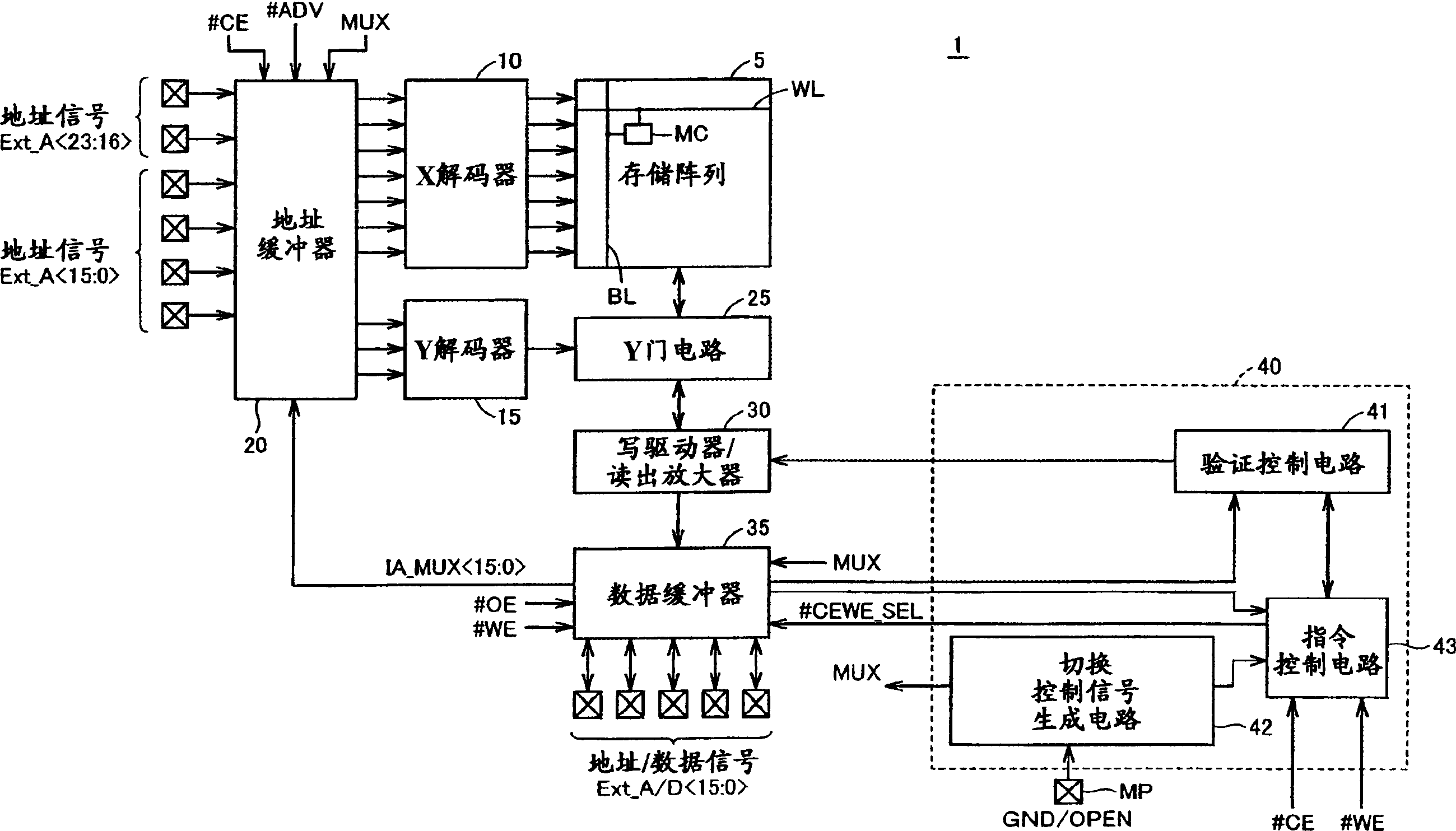
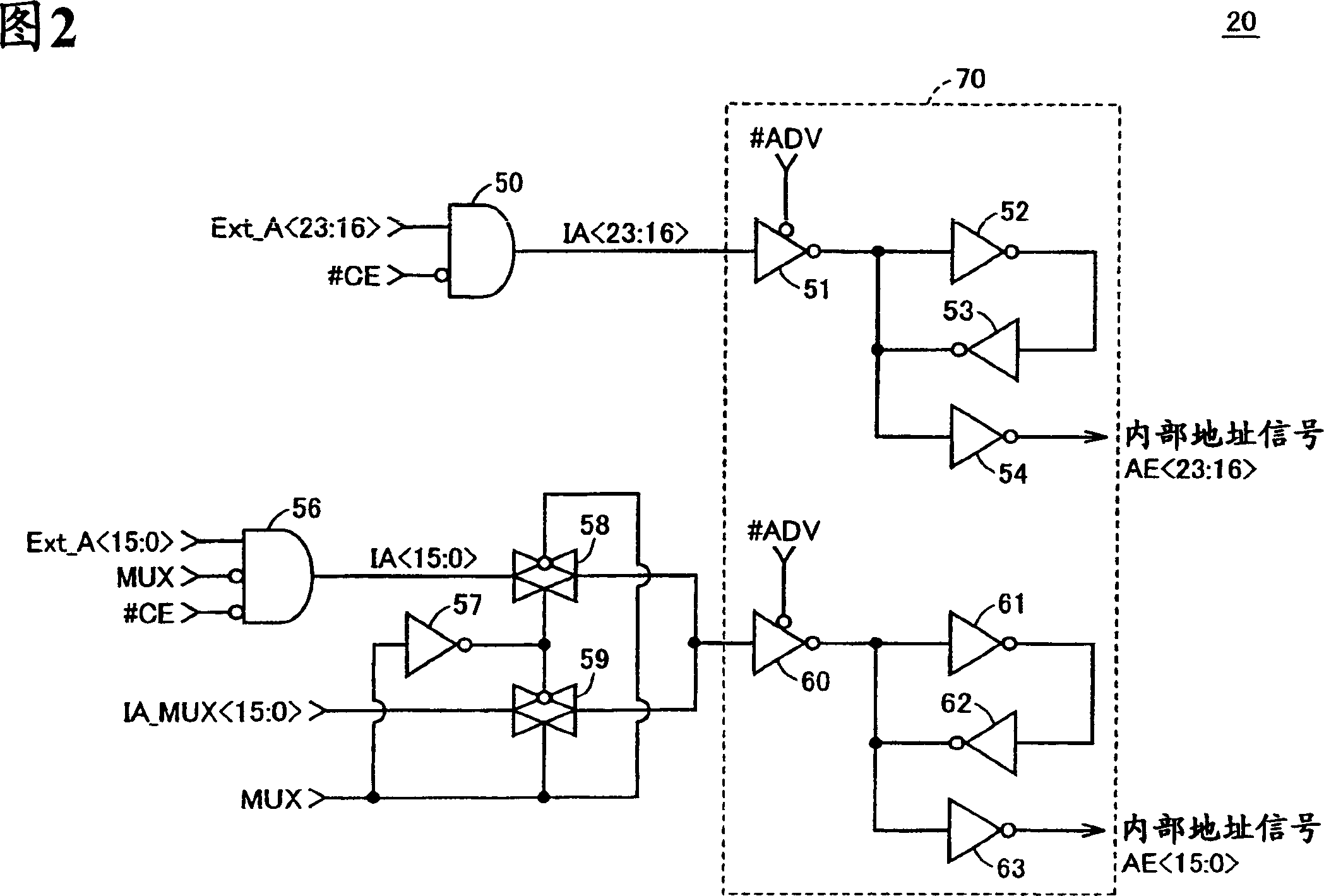
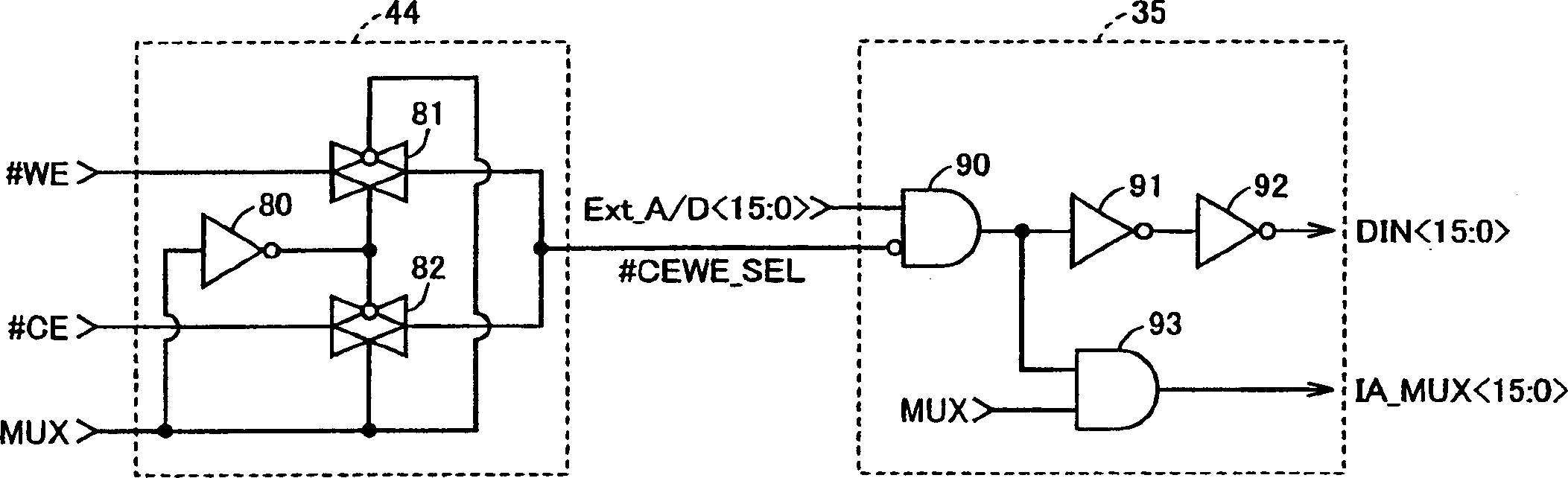
[0021] refer to figure 1 , the semiconductor memory device 1 of the embodiment of the present invention has: a memory array 5 with a plurality of memory cells MC arranged in a matrix (not shown); The X decoder 10 of the word line WL corresponding to the cell row; the Y gate circuit 25 controlling the connection of the bit line BL and the write driver / sense amplifier 30 corresponding to the memory cell column on the column side; The internal address signal of the control Y gate circuit Y decoder 15; According to the address signal input by the address pad (terminal), generate the address buffer 20 of the internal address signal; accept the input from the address data multiplexing pad (terminal) The address / data signal is buffered and output after the input, or the data buffer 35 that receives the input of the read data signal output by the write driver / sense amplifier 30 and outputs it to the address data multiplex pad; the output is used for the control device 1 The control p...
Embodiment 2
[0082] In the above-mentioned first embodiment, regarding the generation of the control signal MUX, a mode in which the pad is connected to the ground voltage GND or set in an open state has been described.
[0083] The second embodiment describes the generation of other control signal MUX.
[0084] refer to Figure 7 , the switching control signal generation circuit 42# and Figure 4 Compared with the switching control signal generation circuit 42 described above, the difference is that the fuse 105 connected to the ground voltage GND is provided instead of the mode pad MP, and the inverter 103 is deleted. Other composition and Figure 4 The switching control signal generation circuit 42 described above is the same, and its detailed description is omitted.
[0085] One end of the fuse 105 is connected to the ground voltage GND, and the other end is connected to the input node of the inverter 101 . Can be cut by laser trimming etc.
[0086] For example, when ...
PUM
 Abstract
Description
Claims
Application Information
 - R&D Engineer
- R&D Manager
- IP Professional
- Industry Leading Data Capabilities
- Powerful AI technology
- Patent DNA Extraction
Browse by: Latest US Patents, China's latest patents, Technical Efficacy Thesaurus, Application Domain, Technology Topic, Popular Technical Reports.
© 2024 PatSnap. All rights reserved.Legal|Privacy policy|Modern Slavery Act Transparency Statement|Sitemap|About US| Contact US: help@patsnap.com