Chip part manufacturing method and chip parts

A manufacturing method and component technology, applied in the manufacture of chip components and the field of chip components, can solve the problems of deformation of chip components, cracks of chip components, application of cutting stress, etc.

Inactive Publication Date: 2012-05-23
PANASONIC CORP
View PDF1 Cites 0 Cited by
  • Summary
  • Abstract
  • Description
  • Claims
  • Application Information

AI Technical Summary

Problems solved by technology

[0008] In the existing structure, in Image 6 In the substrate separation process shown in C, the cutting machine 6 is used to cut between the adjacent substrates 5 by the square cutting method or the Thomson cutting method. cutting width
[0009] Moreover, the first corner formed on the surface vertically intersecting the mounting surface is formed in a right-angled shape. In order to increase the number of cut-out chip components corresponding to the unit area of ​​the printed circuit board 1, if the cutting width of the cutting machine 6 is reduced, It is easy to apply the cutting stress generated by the cutting machine 6 to the chip part 7, causing the disadvantageous situation that the chip part 7 is deformed
[0010] In addition, when a plurality of chip components 7 are supplied to the mounting machine by a feeder or the like, in the case where the chip components come into contact with each other, since the first corners of the chip components 7 are at right angles, the supply cannot be smoothly moved, and Adverse conditions that cause chip components to crack or shatter

Method used


Image

  • Chip part manufacturing method and chip parts
  • Chip part manufacturing method and chip parts
  • Chip part manufacturing method and chip parts

Examples


Embodiment approach 1

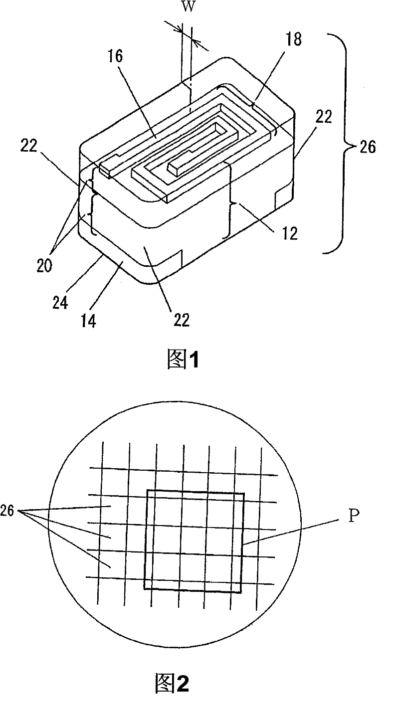
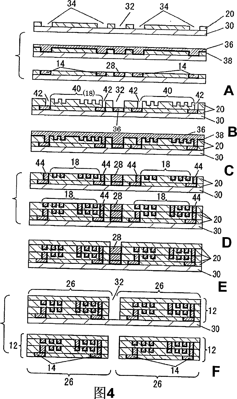
[0033] figure 1 It is a perspective oblique view of the chip part of Embodiment 1, figure 2 is a plan view showing a state in which a plurality of chip components are connected, image 3 yes figure 2 An enlarged top view of part P of . Figure 4 A~ Figure 4 F is a process diagram showing one manufacturing process of the chip component of the present invention.

[0034] exist figure 1 In , there is shown a chip component 26 according to an embodiment of the present invention, for example, a chip coil component. The chip component 26 has a substantially square transparent base 12 , electrodes 14 arranged on the lower surface of the base 12 , and a coil portion 18 formed of a spiral metal layer 16 embedded in the base 12 . The base body 12 is formed by stacking insulating resin layers 20 made of cured photosensitive resin obtained by curing the photosensitive resin.

[0035] In addition, the first corner portion 22 of the chip component 26 is formed in a substantially...

Embodiment approach 2

[0065] Figure 5 A~ Figure 5 G shows another manufacturing process of the chip component 26 of the present invention. Among them, the method used in the first embodiment can also be applied in the second embodiment figure 1 , figure 2 and image 3 , so the detailed description is omitted. Embodiment 2 shows one more manufacturing process than Embodiment 1. Moreover, it is clear at a glance Figure 5 A~ Figure 5 G and Figure 4 A~ Figure 4 F is very similar.

[0066] Figure 5 A shows an electrode forming step. exist Figure 5 In the upper part of A, a release layer (not shown) is formed on one main surface of the substrate 30, and the insulating resin layer 20 having the electrode cavity 34 is formed on the upper portion of the release layer by photolithography. In addition, the lift-off layer can be formed of, for example, a lift-off resist. If the peeling layer is formed, the chip components to be described later can be easily separated in the frame-shaped c...


PUM

PropertyMeasurementUnit
diameteraaaaaaaaaa
heightaaaaaaaaaa
heightaaaaaaaaaa

Abstract

The present invention provides a chip part manufacturing method comprising a separating process capable of suppressing deformation of chip parts, and also provides chip parts. It comprises a step of forming a plurality of frame-like void portions ( 32 ) in one main surface of substrate ( 30 ) and insulating resin layer ( 20 ) having a spiral void portion ( 40 ) disposed in the region thereof, a step of forming metal layer ( 36 ) in frame-like void portion ( 32 ) and spiral void portion ( 40 ) and on insulating resin layer ( 20 ), a step of polishing metal layer ( 36 ) at least up to the uppersurface of insulating resin layer and forming coil section ( 18 ) in spiral void portion ( 40 ), and a step of forming a metal layer for connecting chip parts to frame-like void portion ( 32 ), wherein the metal layer is melted and removed by using an etching agent to separate a plurality of chip parts connected to each other by a frame-like connection.

Description

technical field [0001] This invention relates to the manufacturing method of the chip component used for various electronic equipment etc., and a chip component. Background technique [0002] Figure 6 A~ Figure 6 D is a process diagram showing a conventional manufacturing process of chip components. Figure 7 yes means Figure 6 An exploded oblique view of part S of the chip assembly shown in B. [0003] Figure 6 A. Figure 6 B. Figure 6 C and Figure 6 D is a diagram showing the manufacturing steps of sheet formation, coil portion formation, substrate separation, and electrode formation, respectively. [0004] Such as Figure 6 As shown in A, the sheet forming step forms a plurality of printed circuit boards 1 . Secondly, if Figure 6 B and the following Figure 7 As shown, in the coil portion forming process, arc-shaped conductors 2 are printed on a plurality of printed circuit boards 1 with Ag paste. Then, the printed circuit boards 1 are stacked to form the coil ...

Claims


Application Information

Patent Timeline
Patent Type & Authority Patents(China)
IPC IPC(8): H01F41/00H01F41/04H01F17/00
Inventor 大庭美智央松谷伸哉下山浩司高桥祐一守本慎一
Owner PANASONIC CORP
Why Eureka
Try Eureka