Wafer support member and semiconductor manufacturing system using the same
A technology for supporting members and wafers, which is applied in semiconductor/solid-state device manufacturing, electrical components, circuits, etc., can solve problems such as complex structures, and achieve effective error improvement.
- Summary
- Abstract
- Description
- Claims
- Application Information
AI Technical Summary
Problems solved by technology
Method used
Image
Examples
Embodiment approach 1
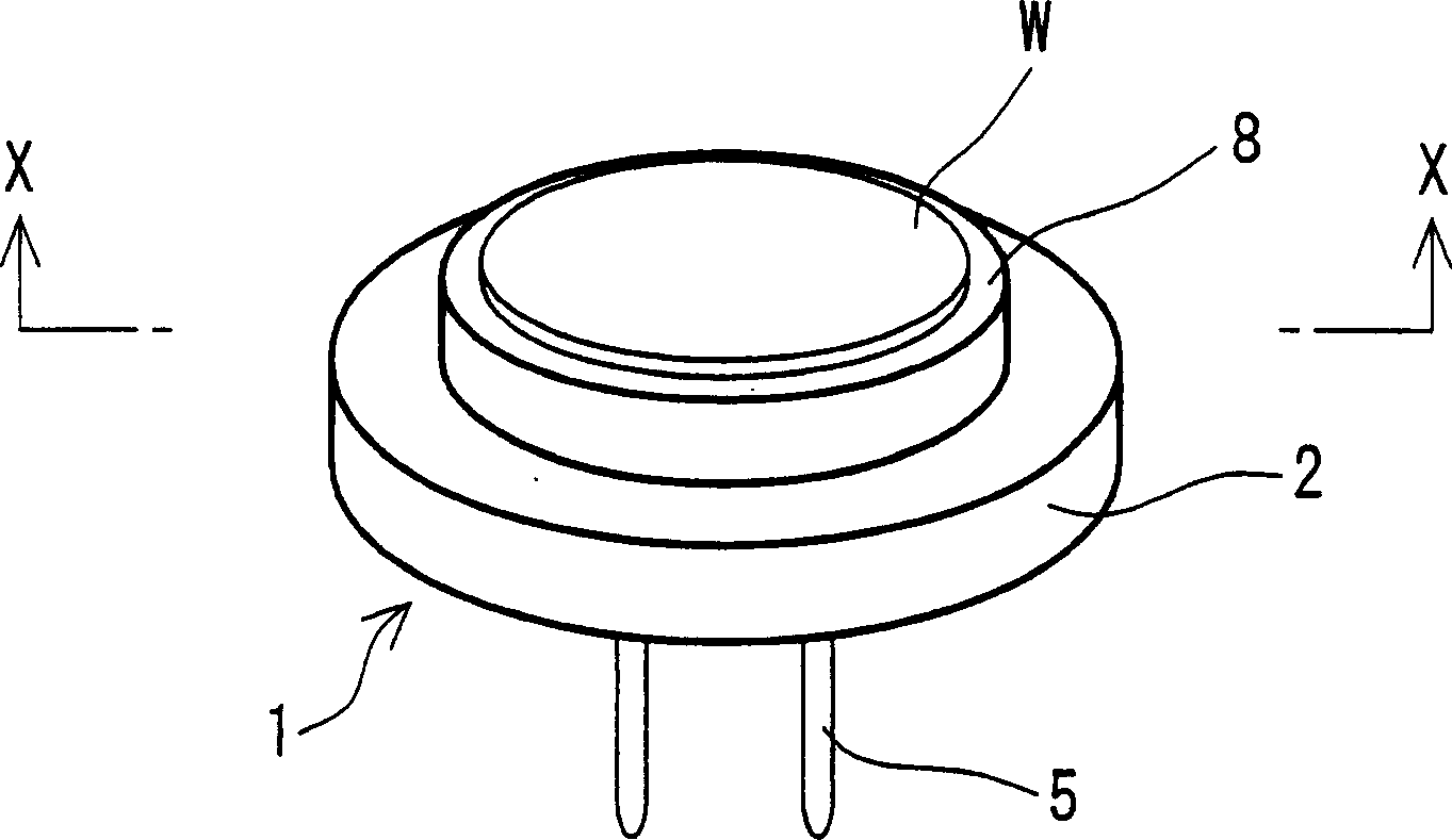
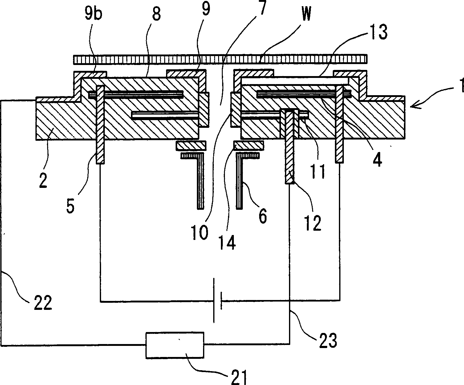
[0047] figure 1 It is a perspective view showing the structure of the wafer support member in Embodiment 1 of this invention. figure 2 yes figure 1 The cross-sectional view of the X-X line.
[0048] Wafer support member 1 according to Embodiment 1 of the present invention includes plate-shaped ceramic body 2 having approximately the same size as wafer W, and one main surface thereof serves as placement surface 8 on which the wafer is placed. Also, a pair of electrostatic adsorption electrodes 4 are buried inside the plate-shaped ceramic body 2, and the power supply terminal 5 for energizing the electrostatic adsorption electrodes 4 is embedded on the other main surface of the plate-shaped ceramic body 2, and the One end of the power supply terminal 5 is exposed. In addition, on the other main surface side of the plate-shaped ceramic body 2 , on the back surface of the wafer W, the conductive pipe 6 for ventilation is bonded to the plate-shaped ceramic body 2 through the ...
Embodiment approach 2
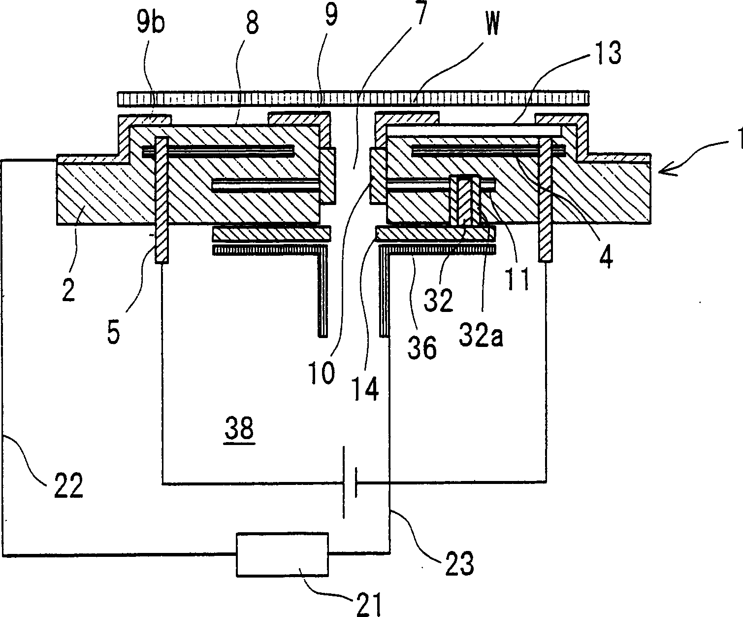
[0057] image 3 , is a perspective view showing an example of a wafer supporting member according to Embodiment 2 of the present invention. In the electrostatic chuck shown in Embodiment 1, one electrode of the resistance meter 21 is connected to the current-carrying terminal 12 through the wire 23. In contrast, in the electrostatic chuck of Embodiment 2, one electrode of the resistance meter 21 is The electrostatic chuck according to Embodiment 2 is different from the electrostatic chuck according to Embodiment 1 in that it is connected to a conductive tube 36 via a wire 23 . Other configurations are the same as those of the electrostatic chuck according to the first embodiment. Due to the above differences, the electrostatic chuck according to the second embodiment is superior to the electrostatic chuck according to the first embodiment in that oxidation of the soldered portion 32 a can be prevented. Hereinafter, the electrostatic chuck according to Embodiment 2 will be de...
Embodiment approach 3
[0066] Figure 4 It is a perspective view showing an example of the wafer support member 1 according to Embodiment 3 of the present invention. The electrostatic chuck shown in Embodiment 2 above, such as image 3 As shown, the conductive pipe 36 to which one electrode of the resistance meter 21 is connected by the wire 23 is connected to the connection conductive layer 10 by the conductive member 32 and the embedded conductive layer 11. In this respect, in the electrostatic chuck according to the third embodiment, Such as Figure 4 As shown, the electrostatic chuck in the third embodiment is different from the electrostatic chuck in the second embodiment in that the conductive tube 46 is connected to the conductive layer 60 directly. Other configurations are the same as those of the electrostatic chuck in the second embodiment. Because of the above-mentioned differences, the electrostatic chuck of Embodiment 3 does not need to make the conductive member 32 and the embedded ...
PUM
 Abstract
Description
Claims
Application Information
 - R&D
- Intellectual Property
- Life Sciences
- Materials
- Tech Scout
- Unparalleled Data Quality
- Higher Quality Content
- 60% Fewer Hallucinations
Browse by: Latest US Patents, China's latest patents, Technical Efficacy Thesaurus, Application Domain, Technology Topic, Popular Technical Reports.
© 2025 PatSnap. All rights reserved.Legal|Privacy policy|Modern Slavery Act Transparency Statement|Sitemap|About US| Contact US: help@patsnap.com


