Wet type cleaning process monitoring apparatus and monitoring method

A monitoring equipment and cleaning technology, applied in the field of monitoring equipment and its monitoring, can solve the problems affecting the company's market competitiveness and share, reducing production capacity, increasing the cost of manufacturing materials, etc.

Inactive Publication Date: 2006-05-10
POWERCHIP SEMICON CORP
View PDF0 Cites 0 Cited by
  • Summary
  • Abstract
  • Description
  • Claims
  • Application Information

AI Technical Summary

Problems solved by technology

[0004] 1. When the existing semiconductor machine cleans the wafer, no warning system is designed to monitor the flow of cleaning water, resulting in serious defects in the automatic production line of the line
[0005] 2. The existing way of cleaning wafers in semiconductor machines requires adding a wafer detection action after the wafer cleaning is completed to ensure that the particles or defects on the wafer surface are within the safe range, thereby increasing the steps required for production and reducing the cost. production capacity
[0006] 3. The existing way of cleaning wafers by semiconductor machines is likely to cause wafer wear and tear, which in turn increases manufacturing costs and affects the company's market competitiveness and share
[0007] 4. The existing method of cleaning wafers by semiconductor machines tends to ignore the particles or defects on the wafer surface that have exceeded the safety range. After the subsequent process steps are completed, the yield rate is reduced or the entire batch is scrapped, which not only consumes time and labor costs, but also And waste material cost, thereby increasing the cost of manufacturing materials and reducing market competitiveness

Method used


Image

  • Wet type cleaning process monitoring apparatus and monitoring method
  • Wet type cleaning process monitoring apparatus and monitoring method
  • Wet type cleaning process monitoring apparatus and monitoring method

Examples


Embodiment Construction

[0035] In order to have a further cognition and understanding of the features, purposes and functions of the present invention, a detailed description is given below with reference to the accompanying drawings.

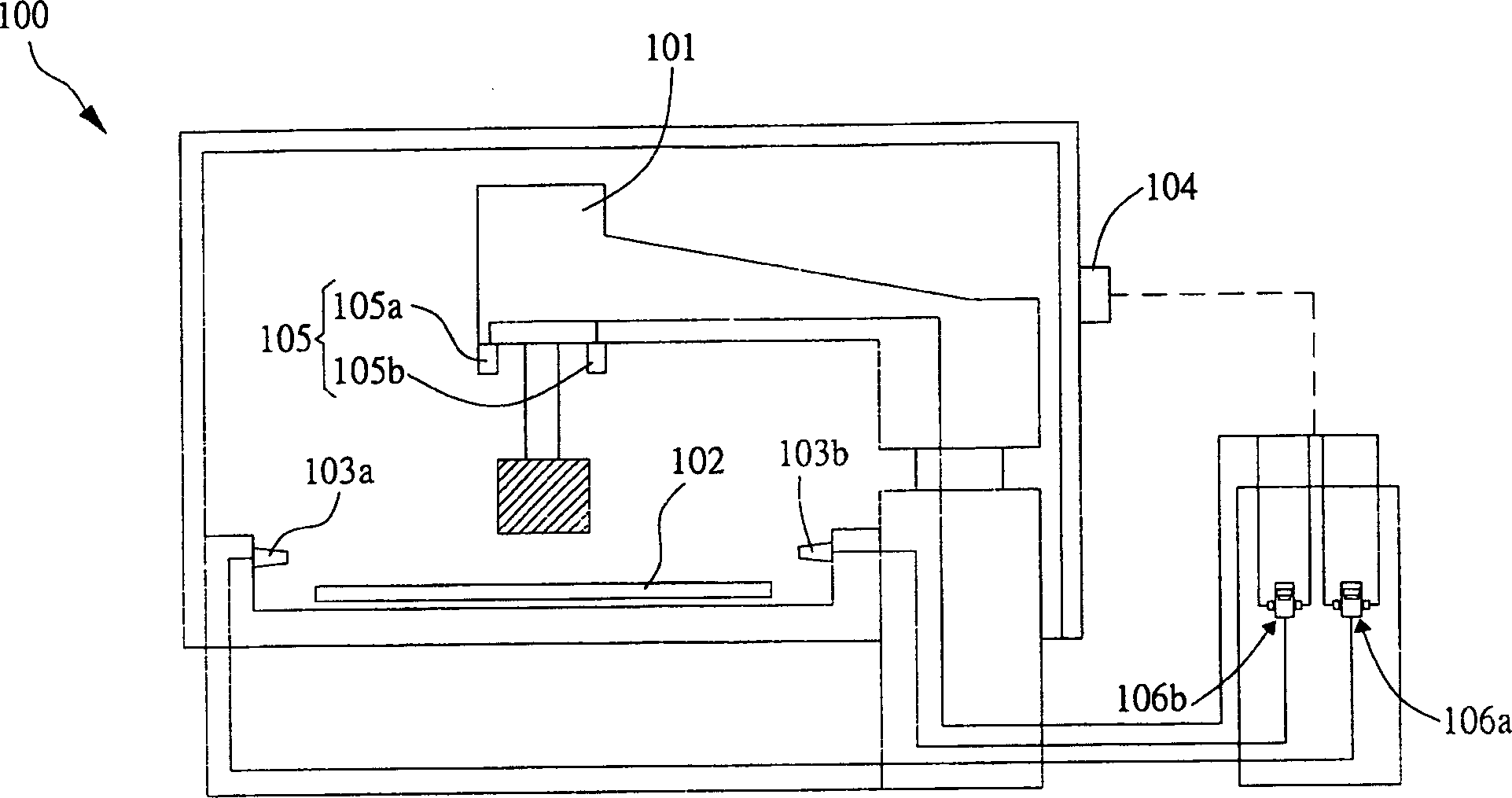
[0036] Such as figure 1 As shown, it is a schematic diagram of a preferred embodiment of the monitoring equipment for the wet cleaning process of the present invention. The wet cleaning equipment 100 is to provide a fluid (not shown) in a cleaning process (usually shown here) to an object to be cleaned. The object referred to is the surface of the wafer 102), and the monitoring device of the present invention is mainly applied in the wet cleaning device 100 having at least one cleaning brush arm 101 and fluid supply units 103a, 103b, and when the cleaning brush arm 101 cleans Wafer 102, the fluid supply unit 103a, 103b also provides fluid on the wafer 102 at the same time, and the monitoring equipment at least includes: an arm position sensor 105 is connected to the c...


PUM


Abstract

This invention relates to one clearing process monitoring device with one clearing arm and one fluid part. When the arm cleans the transistor, the flow provides one fluid part on transistor. The monitor device at least comprises the following parts: arm position sensor connected to arm when the sensor is started; at least one flow sensor unit connected to flow unit to monitor flow providing unit when started. The flow sensor unit at least comprises the following: emission end, receiving end and floating parts, wherein, the receiving end responds to eradiation end to receive signals. The floating element is located between emission end and receiving end. The floating part alters position. The float element makes the receiving end receive the signals from emission end.

Description

technical field [0001] The invention relates to a monitoring device and a monitoring method thereof, in particular to a flow sensing device and method used in a wet cleaning process. Background technique [0002] When the existing semiconductor machine cleans the wafer, it uses the cleaning arm to control the cleaning bristles to clean the wafer, and uses the flow sensor (flow-meter) to control the flow of cleaning water, but the semiconductor machine cleans the wafer. In this method, no warning system is designed. When the flow of cleaning water is too low or the water is short of water, the semiconductor machine will continue to clean the wafer, resulting in dry brushing of the wafer surface, causing the entire wafer to be scrapped and increasing the manufacturing cost. ; and if the online quality control does not find that the particles or defects on the wafer surface have exceeded the safe range after the cleaning is completed, the wafers are sent to the subsequent proce...

Claims


Application Information

Patent Timeline
Patent Type & Authority Applications(China)
IPC IPC(8): H01L21/66B08B3/00G01F23/292H01L21/302H01L21/304
Inventor 吴牧融陈冠名任建国古金山陈其瓒
Owner POWERCHIP SEMICON CORP
Why Eureka
Try Eureka