Plane display device
A flat display, liquid crystal display device technology, applied in static indicators, nonlinear optics, instruments, etc., can solve problems such as pin corrosion, vertical or horizontal line defects, display defects, etc.
- Summary
- Abstract
- Description
- Claims
- Application Information
AI Technical Summary
Problems solved by technology
Method used
Image
Examples
Embodiment 1
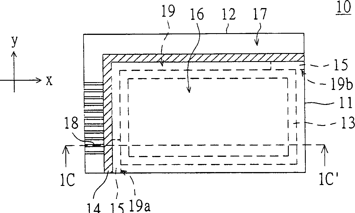
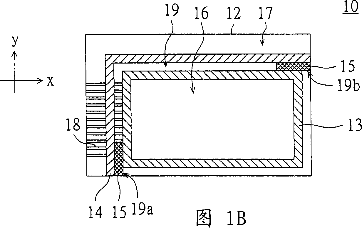
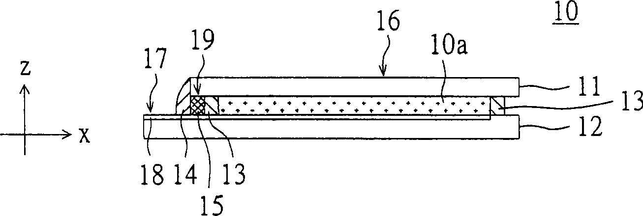
[0031] Please also refer to Figure 1A ~ 1C , Figure 1A The drawing is a top view of a flat panel display device according to an embodiment of the present invention. Figure 1B shows Figure 1A A schematic diagram of the state when the flat panel display device omits the first substrate, Figure 1C drawn along Figure 1A The cross-sectional view of the flat-panel display viewed by the section line 1C-1C'. The flat panel display device 10 of this embodiment may be a liquid crystal display device or an organic light emitting diode (OLED) display device, and a liquid crystal display device is used as an example for illustration here, but the technology of this embodiment is not limited thereto. .
[0032] exist Figure 1A ~ 1C Among them, the flat panel display device 10 at least includes a first substrate 11 , a second substrate 12 , a first sealing material 13 , a second sealing material 14 and a third sealing material 15 . The second substrate 12 is arranged parallel to th...
Embodiment 2
[0041] Please also refer to Figure 2A-2B , Figure 2A A top view showing a flat panel display device according to Embodiment 2 of the present invention, Figure 2B draw Figure 2A A schematic diagram of the state of the flat-panel display device when the first substrate is omitted. The difference between the flat panel display device 20 of the present embodiment and the flat panel display device 10 of the first embodiment lies in the third sealing material 25 , and the same reference numerals are used for the rest of the same components, and the connection relationship and functions between them will not be repeated.
[0042] exist Figure 2A-2B Among them, the third sealing material 25 and the first sealing material 13 that at least seal the first end 19a and the second end 19b of the gap 19 can be integrally formed, for example, the materials of the first sealing material 13 and the third sealing material 25 All are silicone. In addition, the third sealing material 25 ...
Embodiment 3
[0044] Please also refer to Figure 3A-3B , Figure 3A A top view showing a flat panel display device according to Embodiment 3 of the present invention, Figure 3B is shown along the Figure 3A The cross-sectional view of the flat-panel display viewed by the section line 3B-3B'. The difference between the flat-panel display device 30 of the present embodiment and the flat-panel display device 10 of the first embodiment lies in the third sealing material 35 and the second sealing material 34, and the rest of the same constituent elements continue to use the reference numerals, and the relationship between them will not be repeated. connections and functions.
[0045] exist Figure 3A-3B Among them, the second sealing material 34 is disposed around the surface edge of the first substrate 11 , so that the third sealing material 35 that at least seals the first end 19 a and the second end 19 b of the gap 19 is a part of the second sealing material 34 . Wherein, the second se...
PUM
 Abstract
Description
Claims
Application Information
 - R&D
- Intellectual Property
- Life Sciences
- Materials
- Tech Scout
- Unparalleled Data Quality
- Higher Quality Content
- 60% Fewer Hallucinations
Browse by: Latest US Patents, China's latest patents, Technical Efficacy Thesaurus, Application Domain, Technology Topic, Popular Technical Reports.
© 2025 PatSnap. All rights reserved.Legal|Privacy policy|Modern Slavery Act Transparency Statement|Sitemap|About US| Contact US: help@patsnap.com


